2. Analog video
Input
CVBS / COMPONENT
A
Is the power voltage being output correctly?
SIDE CNT PCB
V+5V : [CN28B : 1pin]
V-5V : [CN28B : 5 pin]
Check of the I2C control signal for video selector
IC [IC511].
DIGITAL PCB
I2C(SCL) : [BN21A : 5 pin] (AVSCL)
I2C(SDA) : [BN21A : 4 pin] (AVSDA)
See "I2C communication wave form (sample)"
Does the signal input to the video decoder
[IC351]?
DIGITAL PCB
V : [R3526]
COMPONENT-Y : [R3527]
COMPONENT-Cb : [R3528]
COMPONENT-Cr : [R3529]
· SIDE CNT PCB [BN77D] connection is faulty.
· REGULATOR (SPEAKER) PCB faulty.
DIGITAL PCB faulty.
· FRONT CNT board is faulty or inserted incor-
rectly.
[CN21A]
VIDEO PCB faulty. ⇒ TO "B"
· CVBS Monitor Out is NG
COMPONENT Monitor Out is NG ⇒ To "B"
· HDMI Out is NG ⇒ TROUBLE SHOOTING To "3. HDMI/DVI"
MONITOR OUT (CVBS / COMPONENT / HDMI OUT NG
To "A"
Input CVBS
Perform the operation below beforehand.
b
Check it whether connection cable and Monitor are normal.
b
VIDEO Convert is set to ON.
b
Setting as follows.
V : SAT
COMPONENT : DVD
Input COMPONENT
NO
NO
NO
YES
YES
YES
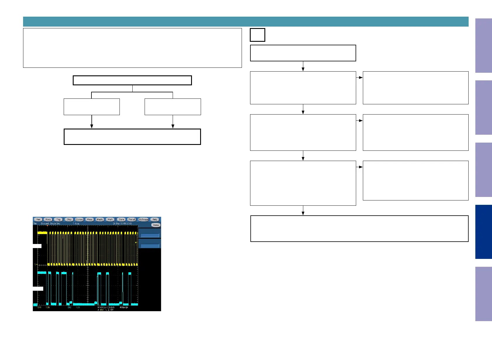
I2C communication wave form (sample)
CLK
DATA
Before Servicing
This Unit
Electrical Mechanical Repair Information Updating
90

 Loading...