FUNCTIONAL BLOCK DIAGRAM
[AK4490]
MS1648-J-03 2014/11
- 7 -
16 DEM1 I De-emphasis Enable 1 Pin in Parallel Control Mode (Internal pull-down pin)
17
ACKS I Master Clock Auto Setting Mode Pin in Parallel Mode (Internal pull-down pin)
CAD1 I Chip Address 1 Pin in Serial Control Mode
18 NC -
No internal bonding.
Connect to GND.
19 VREFHR I Rch High Level Voltage Reference Input Pin
20 VREFHR I Rch High Level Voltage Reference Input Pin
21 VREFLR I Rch Low Level Voltage Reference Input Pin
21 VREFLR I Rch Low Level Voltage Reference Input Pin
23 VCMR -
Right channel Common Voltage Pin,
Normally connected to VREFLR with a 10uF electrolytic cap.
24 NC -
No internal bonding.
Connect to GND.
25 AOUTRP O Rch Positive Analog Output Pin
26 AOUTRN O Rch Negative Analog Output Pin
27 VDDR - Rch Analog Power Supply Pin, 4.75 7.2V
28 VDDR - Rch Analog Power Supply Pin, 4.75 7.2V
29 VSSR Ground Pin
30 VSSR Ground Pin
31 VSSL Ground Pin
32 VSSL Ground Pin
33 VDDL - Lch Analog Power Supply Pin, 4.75 7.2V
34 VDDL - Lch Analog Power Supply Pin, 4.75 7.2V
35 AOUTLN O Lch Negative Analog Output Pin
36 AOUTLP O Lch Positive Analog Output Pin
37 NC -
No internal bonding.
Connect to GND.
38 VCML -
Left channel Common Voltage Pin,
Normally connected to VREFLL with a 10uF electrolytic cap.
39 VREFLL I Lch Low Level Voltage Reference Input Pin
40 VREFLL I Lch Low Level Voltage Reference Input Pin
41 VREFHL I Lch High Level Voltage Reference Input Pin
42 VREFHL I Lch High Level Voltage Reference Input Pin
43 NC -
No internal bonding.
Connect to GND.
44 AVDD - Analog Power Supply Pin, 3.0 3.6V
45 AVSS - Ground Pin
46 MCLK I Master Clock Input Pin
47 DVSS - Ground Pin
48 DVDD - Digital Power Supply Pin, 3.0 3.6V
Note: All input pins except internal pull-up/down pins must not be left floating.
DAC
VOUT1
DAC
VOUT2
DAC
VOUT3
DAC
VOUT4
DAC
VOUT5
DAC
VOUT6
AGND2
VDD
DGND
VCOM
VCC1
AGND1
VCC2
DAC
VOUT7
DAC
VOUT8
DigitalFilter
and
Volume
PowerSupplyand
CommonVoltage
SCKI
SCKManager
RST
AMUTEO
AMUTEI
ZERO2
ZERO1
MODE
MD/SDA/DEMP
MC/SCL/FMT
MS/ADR0/RSV
ControlInterface
(SPI/I C/HW)
2
LRCK
BCK
DIN4
DIN3
DIN2
DIN1
AudioInterface
PCM1690
SBAS448A– OCTOBER 2008 – REVISED JANUARY 2009..............................................................................................................................................
www.ti.com
8 Submit Documentation Feedback Copyright © 2008–2009, Texas Instruments Incorporated
Product Folder Link(s): PCM1690
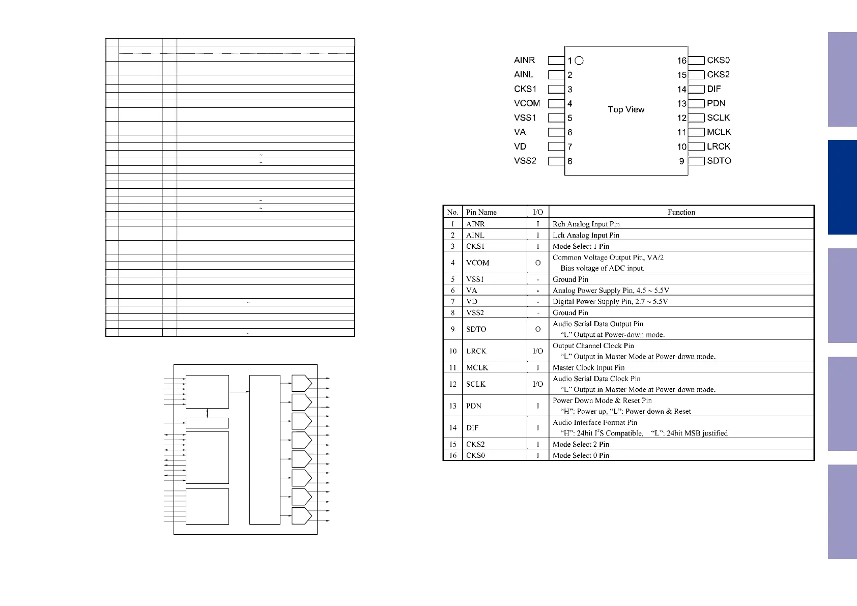
AK5358BET (DAC : U5001)
AK5358BET Pin Function
Before Servicing
This Unit
Electrical Mechanical Repair Information Updating
64

 Loading...