EasyManua.ls Logo

Denon DCD-SA100 User Manual

Denon DCD-SA100
87 pages
To Next Page IconTo Next Page
Page #1 background imageLoading...
Page #1 background image
SERVICE MANUAL
SUPER AUDIO CD PLAYER
MODEL DCD-SA100
For Japan model
16-11, YUSHIMA 3-CHOME, BUNKYOU-KU, TOKYO 113-0034 JAPAN
S-1130V.01 DE/CDM 0307
Some illustrations using in this service manual are
slightly different from the actual set.
Please use this service manual with referring to the
operating instructions without fail.
For purposes of improvement, specifications and
design are subject to change without notice.
本文中に使用しているイラストは、説明の都合上現物
と多少異なる場合があります。
修理の際は、必ず取扱説明書を参照の上、作業を行っ
てください。
サービスをおこなう前に、このサービスマニュアルを
必ずお読みください。本機は、火災、感電、けがなど
に対する安全性を確保するために、さまざまな配慮を
おこなっており、また法的には「電気用品安全法」に
もとづき、所定の許可を得て製造されております。
従ってサービスをおこなう際は、これらの安全性が維
持されるよう、このサービスマニュアルに記載されて
いる注意事項を必ずお守りください。
本機の仕様は性能改良のため、予告なく変更すること
があります。
補修用性能部品の保有期間は、製造打切後8年です。
注 意
Ver. 1
w
w
w
.
x
i
a
o
y
u
1
6
3
.
c
o
m
Q
Q
3
7
6
3
1
5
1
5
0
9
9
2
8
9
4
2
9
8
T
E
L
1
3
9
4
2
2
9
6
5
1
3
9
9
2
8
9
4
2
9
8
0
5
1
5
1
3
6
7
3
Q
Q
TEL 13942296513 QQ 376315150 892498299
http://www.xiaoyu163.com
Question and Answer IconNeed help?

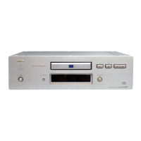
Do you have a question about the Denon DCD-SA100 and is the answer not in the manual?

Denon DCD-SA100 Specifications

General IconGeneral
BrandDenon
ModelDCD-SA100
CategoryCar Stereo System
LanguageEnglish

Summary

General Safety and Service Precautions

Service Manual Guidelines

Guidelines for service personnel including safety warnings and product improvement notes.

Safety Precautions for Service Operations

Electrical Safety and Component Handling

Covers electrical shock prevention, using specified parts, and correct installation.

Leakage Current and Laser Safety Checks

Procedures for leakage current checks, laser safety, and post-service insulation checks.

Laser Pickup Handling and Replacement

Precautions for Disassembly, Storage, and Handling

Guidelines on avoiding disassembly, proper storage, and careful handling of the laser pickup mechanism.

Laser Pickup Component and Environment Precautions

Care for Optical Components and Environment

Instructions for cleaning optical lenses, preventing static discharge, and avoiding corrosive environments.

Laser Drive Circuit Protection

Safety measures for the laser drive circuit, including protection against static electricity.

Optical Pickup Diagnostics and Replacement

Pickup Replacement Criteria and Procedure

Diagnosing pickup failure and the process for replacing the traverse unit, including current registration.

SACD Mechanism and Laser Pickup Procedures

Laser Pickup Replacement and Lop Measurement

Procedure for replacing the laser pickup and method for measuring laser drive current (lop).

Laser Current Measurement Procedures

DVD and CD Laser Current Measurement

Detailed steps for measuring DVD and CD laser currents using an oscilloscope.

Traverse Unit Replacement Method

Traverse Unit Replacement Steps

Preparation, removal, and installation procedures for the traverse unit.

Assembly Procedures

Assembly Steps (1-3): Pickup, Clamp Base, and Damper

Covers pickup short removal, clamp base installation, and damper mounting.

Manual Tray Operation

Manual Tray Opening Procedure

Steps to manually open the disc tray when electronic controls fail.

CD Test and Service Mode Operations

CD Test/Service Mode Flowchart

Flowchart illustrating the sequence of operations and modes in CD test and service modes.

Test Mode Setup Procedures

Entering, Selecting, and Deciding Test Modes

How to enter test mode, select modes, and confirm the selected mode.

Advanced Test Mode Operations

Trace Mode Details and Execution

Details and execution of trace mode for error rate display.

Other Test Mode Functions

Returning to initial state, servo readjustment, and heat-run mode entry.

Test Mode Parameter Tables

Table 1: Servo Adjustment Value Display Mode

Details of servo adjustment parameters and their meanings in test mode.

Trace Mode Parameter Tables

Table 2: Trace Mode Details

Details on trace mode parameters like error detection numbers and addresses.

Disc Information Tables

Table 3: Disc Distinction Information

Data for distinguishing between different disc types based on measured parameters.

Table 4: Disc Classification Information

Table mapping disc types to their media codes.

System Block Diagram

FGSA100 Block Diagram Overview

Overall block diagram of the FGSA100 unit showing major ICs and their interconnections.

Semiconductor IC Information

Integrated Circuit Pin Assignments

Pin assignment diagrams for key semiconductor ICs like CXD1885Q.

IC Functions and Interface Details

MCU Interface Terminal Functions

Description of MCU interface terminals, their properties, and functions.

CXD2753R IC Details

CXD2753R Pin Assignment and Block Diagram

Pin configuration and internal block diagram for the CXD2753R IC.

Microcontroller Interface Terminal Functions

Microcontroller Pin Definitions and Functions

Detailed definitions for microcontroller interface pins and their associated functions.

M30624FGNGP IC Pin Assignment

M30624FGNGP Microcontroller Pinout

Pin assignment diagram for the M30624FGNGP microcontroller.

M30624FGNGP Port Assignment

M30624FGNGP Port Details and Functions

Detailed port assignments, modes, and functions for the M30624FGNGP.

ML9207-01 FL Display IC Details

ML9207-01 Pin Assignment and Terminal Functions

Pin assignment and terminal function descriptions for the ML9207-01 FL display driver.

CXD1881AR IC Pin Assignment

CXD1881AR RF Amplifier Pinout

Pin assignment diagram for the CXD1881AR RF amplifier.

CXD1881AR Internal Block Diagram

CXD1881AR Functional Blocks and Signals

Internal block diagram of the CXD1881AR showing signal paths and functional units.

CXD1881AR Terminal Functions

CXD1881AR Power, Input, and Output Pins

Description of power supply, input, and output pins for the CXD1881AR IC.

CXD1881AR Analog and Serial Port Pins

Analog and Serial Port Pin Functions

Functions of analog and serial port pins for the CXD1881AR IC.

16M SDRAM IC Details

16M SDRAM Terminal Functions

Terminal functions for the 16M SDRAM IC, including power, address, and data pins.

FAN8042 Motor Driver IC Details

FAN8042 Pin Assignment Diagram

Pin assignment diagram for the FAN8042 motor driver IC.

FAN8042 Pin Definitions

FAN8042 Pin Descriptions and Functions

Detailed definitions and functions for all pins of the FAN8042 IC.

FAN8042 Internal Block Diagram

FAN8042 Functional Blocks and Circuits

Block diagram illustrating the internal circuits and connections of the FAN8042 IC.

DXP7001AF IC Functions

DXP7001AF Terminal Functions Description

Description of terminal functions for the DXP7001AF IC, including data and clock signals.

M11L16161SA Memory IC Details

M11L16161SA Pin Assignment and Descriptions

Pin assignment and detailed descriptions for the M11L16161SA memory IC.

AN8471SA Motor Driver IC Details

AN8471SA Pin Assignment and Functions

Pin assignment and functional descriptions for the AN8471SA motor driver IC.

Memory and DSD IC Details

T14L1024N Memory IC Pin Assignment

Pin assignment diagram for the T14L1024N memory IC.

DSD1792DBR Terminal Functions

Description of terminal functions for the DSD1792DBR IC, including audio data and clock signals.

Specific ICs and Transistors

Miscellaneous IC Pin Assignments

Pin assignments and configurations for various ICs like TC74VHC157, AT24C04, S-80843C.

Transistor Specifications and Diagrams

Specifications and circuit diagrams for DTA114EK (PNP) and DTC114EK (NPN) transistors.

FL Display Unit Information

FL Display Pin Connections and Assignments

Diagrams showing FL display pin connections, grid assignments, and anode connections.

Printed Wiring Board (PWB) Layouts

CD/SACD PWB Component Layout

Component layout diagram for the 1U-3532 CD/SACD PWB unit.

Power/Display PWB Layout

1U-3533 Power/Display PWB Component Layout

Component layout diagram for the 1U-3533 Power/Display PWB unit.

SACD Module PWB Layout

1U-3562 SACD Module PWB Component Layout

Component layout diagram for the 1U-3562 SACD Module PWB unit.

Parts List Conventions and Component Details

Parts List Notes and Ordering Information

Notes on parts list usage, ordering, markings, and conventions for resistors and capacitors.

PWB Parts List (CD/SACD)

Semiconductor and Resistor Components for CD/SACD PWB

Lists of semiconductor devices and resistors used on the CD/SACD PWB.

Exploded View of Main Assembly

Main Assembly Parts List

List of parts for the main assembly, referenced by numbers in the exploded view diagram.

Exploded View Parts List (CD/SACD Mechanism)

CD/SACD Mechanism Components

List of chassis, plates, gears, motors, and accessories for the CD/SACD mechanism.

CD/SACD Mechanism Screws and Tapes

List of screws, tapes, and connectors used in the CD/SACD mechanism.

Exploded View of SACD Mechanism

SACD Mechanism Parts List

List of parts for the SACD mechanism, referenced by numbers in the exploded view diagram.

SACD Mechanism Components

SACD Mechanism Semiconductor and Resistor Lists

Lists of semiconductor devices and resistors specific to the SACD mechanism.

Greasing Points Diagram (Part 1)

SACD Mechanism Greasing Instructions (1/2)

Diagram showing greasing points on the SACD mechanism with grease specifications.

Greasing Points Diagram (Part 2)

SACD Pickup Greasing Instructions (2/2)

Diagram showing greasing points on the SACD pickup unit with grease specifications.

Packing View and Accessories

Packing Components and Accessories List

Diagram of packing materials and list of packing/accessories, including cushions and cords.

Waveform Diagrams

SACD Module and Junction Unit Waveforms

Waveform diagrams illustrating signals within the SACD module and Junction unit.

Playback and Disc Operation Waveforms

Playback Waveform Analysis (CD/SACD)

Waveforms for playback and disc detection signals during CD and SACD operation.

Focus Inject and Playback Start Waveforms

Waveforms for focus inject and playback start signals during CD/SACD operation.

Loader Operation Waveforms

Loader Open/Close Operation Waveforms

Waveforms illustrating the loader mechanism's open and close operations.

Schematic Diagram Notes

Notes on Schematic Diagrams and Component Values

Important notes regarding schematic diagrams, warnings, and conventions for component values.

Schematic Diagrams (Part 1 of 7)

Schematic Diagrams (1/7)

First part of the system schematic diagrams.

Schematic Diagrams (Part 2 of 7)

Schematic Diagrams (2/7)

Second part of the system schematic diagrams.

Schematic Diagrams (Part 3 of 7)

Schematic Diagrams (3/7)

Third part of the system schematic diagrams.

Schematic Diagrams (Part 4 of 7)

Schematic Diagrams (4/7)

Fourth part of the system schematic diagrams.

Schematic Diagrams (Part 5 of 7)

Schematic Diagrams (5/7)

Fifth part of the system schematic diagrams.

Schematic Diagrams (Part 6 of 7)

Schematic Diagrams (6/7)

Sixth part of the system schematic diagrams.

Schematic Diagrams (Part 7 of 7)

Schematic Diagrams (7/7)

Final part of the system schematic diagrams.