55
M29W640GB70NA6E (MAIN : IC501)
M29W640GB70NA6E Pin Description
48
8.2 IC DATA
Q101 : M29W640GB70NA
Q101 : M29W640GB70NA
Description M29W640GH, M29W640GL, M29W640GT, M29W640GB
8/90
The M29W640G has an extra block, the extended block, of 128 words in x16 mode or of
256 bytes in x8 mode that can be accessed using a dedicated command. The extended
block can be protected and so is useful for storing security information. However the
protection is not reversible, once protected the protection cannot be undone.
The M29W640GT, M29W640GB, M29W640GH and M29W640GL, are offered in TSOP48
(12 x 20 mm), TSOP56 (14 x 20 mm), TFBGA48 (6 x 8 mm, 0.8 mm pitch), and TBGA64
(10 x 13 mm, 1 mm pitch) packages.
The memory is delivered with all the bits erased (set to ‘1’).
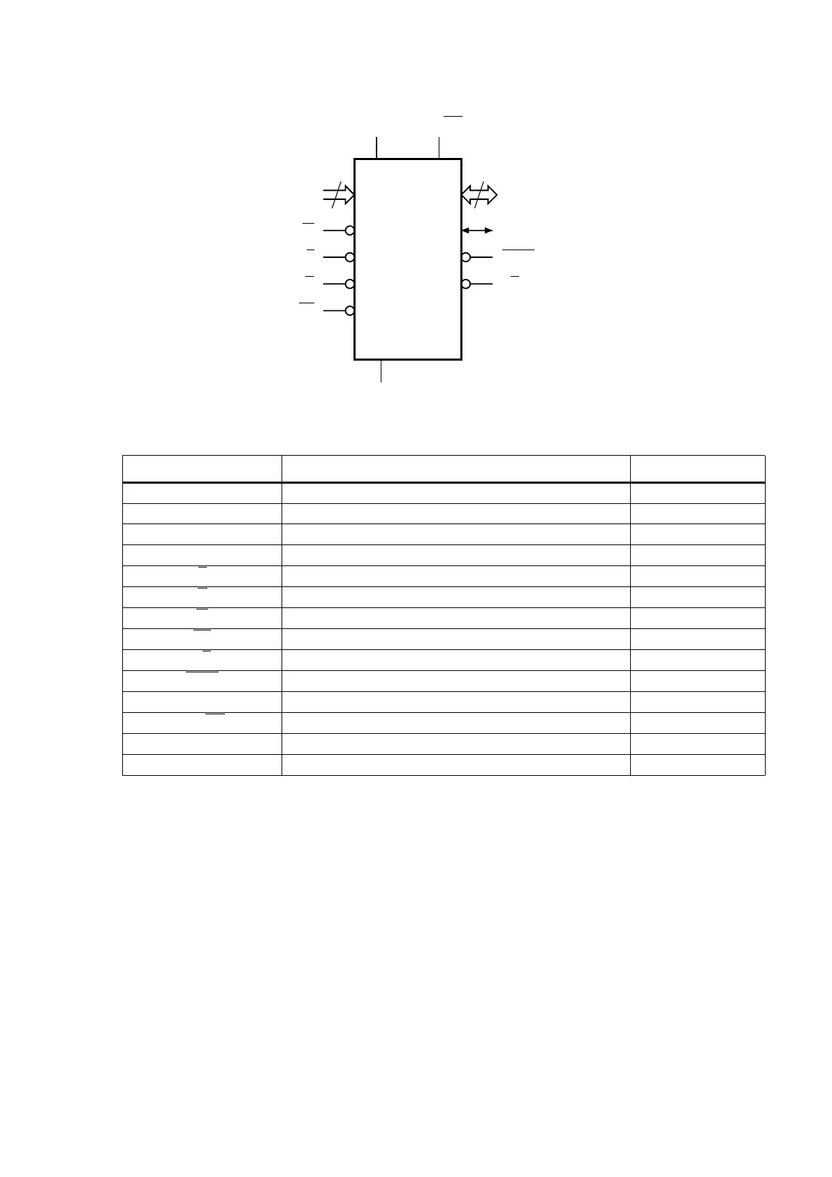
Figure 1. Logic diagram
ai13694
22
A0-A21
W
DQ0-DQ14
V
CC
M29W640GT
M29W640GB
M29W640GH
M29W640GL
E
V
SS
15
G
RP
DQ15A–1
BYTE
RB
V
PP
/WP
Table 2. Signal names
(1)
Name Description Direction
A0-A21 Address Inputs Inputs
DQ0-DQ7 Data Inputs/Outputs Inputs/Outputs
DQ8-DQ14 Data Inputs/Outputs Inputs/Outputs
DQ15A–1 (or DQ15) Data Input/Output or Address Input (or Data Input/Output) Inputs/Outputs
E
Chip Enable Input
G
Output Enable Input
W
Write Enable Input
RP
Reset/Block Temporary Unprotect Input
RB
Ready/Busy Output
BYTE
Byte/Word Organization Select Input
V
CC
Supply voltage Supply voltage
V
PP
/WP Supply voltage for fast program (optional) or write protect Supply voltage
V
SS
Ground –
NC Not connected internally –
1. V
PP
/WP may be left floating since it is internally connected to an pull-up resistor to enable program/erase operations,
Description M29W640GH, M29W640GL, M29W640GT, M29W640GB
8/90
The M29W640G has an extra block, the extended block, of 128 words in x16 mode or of
256 bytes in x8 mode that can be accessed using a dedicated command. The extended
block can be protected and so is useful for storing security information. However the
protection is not reversible, once protected the protection cannot be undone.
The M29W640GT, M29W640GB, M29W640GH and M29W640GL, are offered in TSOP48
(12 x 20 mm), TSOP56 (14 x 20 mm), TFBGA48 (6 x 8 mm, 0.8 mm pitch), and TBGA64
(10 x 13 mm, 1 mm pitch) packages.
The memory is delivered with all the bits erased (set to ‘1’).
Figure 1. Logic diagram
ai13694
22
A0-A21
W
DQ0-DQ1
V
CC
M29W640GT
M29W640GB
M29W640GH
M29W640GL
E
V
SS
15
G
RP
DQ15A–1
BYTE
RB
V
PP
/WP
Table 2. Signal names
(1)
Name Description Direction
A0-A21 Address Inputs Inputs
DQ0-DQ7 Data Inputs/Outputs Inputs/Outputs
DQ8-DQ14 Data Inputs/Outputs Inputs/Outputs
DQ15A–1 (or DQ15) Data Input/Output or Address Input (or Data Input/Output) Inputs/Outputs
E
Chip Enable Input
G
Output Enable Input
W
Write Enable Input
RP
Reset/Block Temporary Unprotect Input
RB
Ready/Busy Output
BYTE
Byte/Word Organization Select Input
V
CC
Supply voltage Supply voltage
V
PP
/WP Supply voltage for fast program (optional) or write protect Supply voltage
V
SS
Ground –
NC Not connected internally –
1. V
PP
/WP may be left floating since it is internally connected to an pull-up resistor to enable program/erase operations,
48
8.2 IC DATA
Q101 : M29W640GB70NA
Q101 : M29W640GB70NA
Description M29W640GH, M29W640GL, M29W640GT, M29W640GB
8/90
The M29W640G has an extra block, the extended block, of 128 words in x16 mode or of
256 bytes in x8 mode that can be accessed using a dedicated command. The extended
block can be protected and so is useful for storing security information. However the
protection is not reversible, once protected the protection cannot be undone.
The M29W640GT, M29W640GB, M29W640GH and M29W640GL, are offered in TSOP48
(12 x 20 mm), TSOP56 (14 x 20 mm), TFBGA48 (6 x 8 mm, 0.8 mm pitch), and TBGA64
(10 x 13 mm, 1 mm pitch) packages.
The memory is delivered with all the bits erased (set to ‘1’).
Figure 1. Logic diagram
ai13694
22
A0-A21
W
DQ0-DQ1
V
CC
M29W640GT
M29W640GB
M29W640GH
M29W640GL
E
V
SS
15
G
RP
DQ15A–1
BYTE
RB
V
PP
/WP
Table 2. Signal names
(1)
Name Description Direction
A0-A21 Address Inputs Inputs
DQ0-DQ7 Data Inputs/Outputs Inputs/Outputs
DQ8-DQ14 Data Inputs/Outputs Inputs/Outputs
DQ15A–1 (or DQ15) Data Input/Output or Address Input (or Data Input/Output) Inputs/Outputs
E
Chip Enable Input
G
Output Enable Input
W
Write Enable Input
RP
Reset/Block Temporary Unprotect Input
RB
Ready/Busy Output
BYTE
Byte/Word Organization Select Input
V
CC
Supply voltage Supply voltage
V
PP
/WP Supply voltage for fast program (optional) or write protect Supply voltage
V
SS
Ground –
NC Not connected internally –
1. V
PP
/WP may be left floating since it is internally connected to an pull-up resistor to enable program/erase operations,
 Loading...