64
PLL1707DBQ (MAIN : IC402)
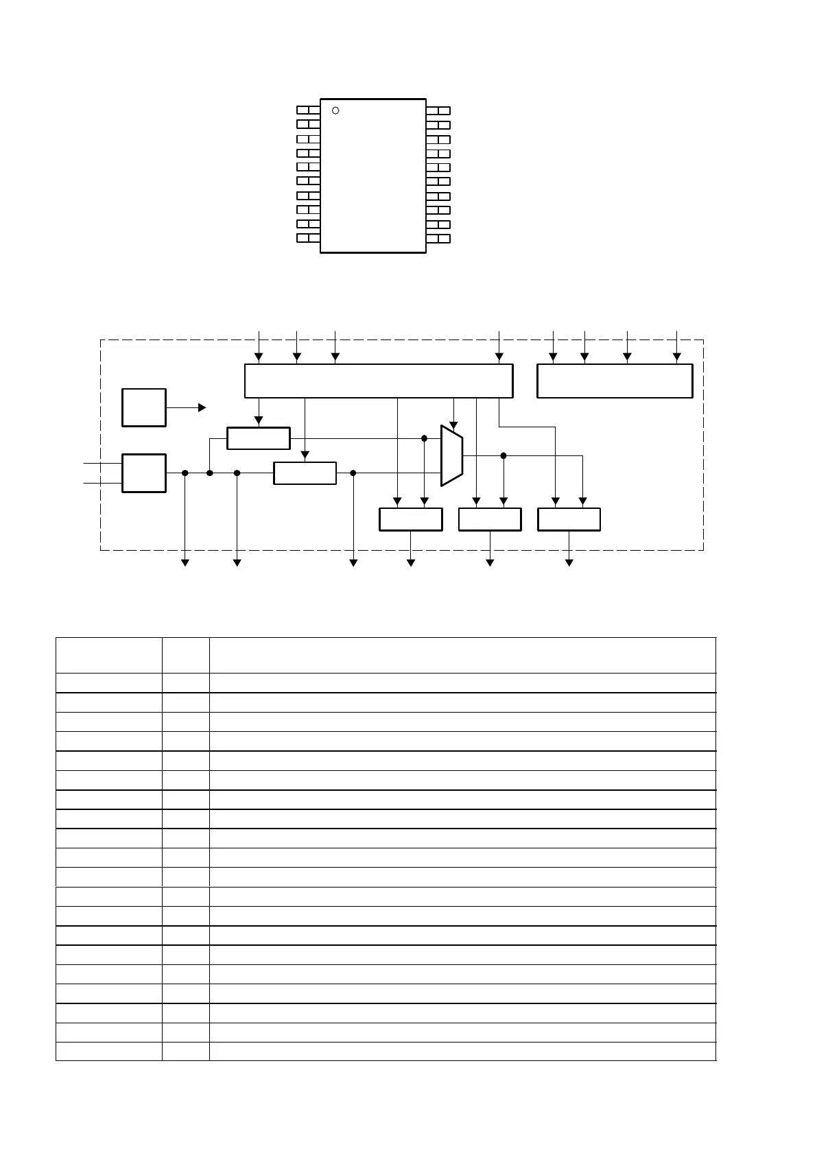
PLL1707DBQ Block Diagram
PLL1707DBQ Pin Function
SLES065 – DECEMBER 2002
www.ti.com
4
ELECTRICAL CHARACTERISTICS (continued)
all specifications at T
A
= 25°C, V
DD
1–V
DD
3 (= V
DD
) = V
CC
= 3.3 V, f
M
= 27 MHz, crystal oscillation, f
S
= 48 kHz (unless otherwise noted)
PARAMETER UNITMAXTYPMINTEST CONDITIONS
SCKO0, SCKO1 58 100 ps
Output clock jitter
Frequency Settling Time
(7)
PLL1707, to stated output frequency 50 150
PLL1708, to stated output frequency 80 300
ns
Power-up time
(8)
To stated output frequency 3 6 ms
POWER SUPPLY REQUIREMENTS
V
CC
, V
DD
Supply voltage range 2.7 3.3 3.6 Vdc
V
DD
= V
CC
= 3.3 V, f
S
= 48 kHz 19 25 mA
I
DD
+ I
CC
Supply current
Power down
(10)
350 550 µA
Power dissipation V
DD
= V
CC
= 3.3 V, f
S
= 48 kHz 63 90 mW
TEMPERATURE RANGE
Operating temperature –25 85 °C
θ
JA
Thermal resistance PLL1707/8DBQ: 20-pin SSOP (150 mil) 150 °C/W
(1)
Pins 5, 6, 7, 12: FS1/MD, FS2/MC, SR/MS, CSEL (Schmitt-trigger input with internal pulldown, 3.3-V tolerant)
(2)
Pins 2, 3, 14, 15, 18, 19: SCKO2, SCKO3, MCKO1, MCKO2, SCKO0, SCKO1
(3)
Pin 10: XT1
(4)
Pin 11: XT2
(5)
Jitter performance is specified as standard deviation of jitter for 27-MHz crystal oscillation and default SCKO frequency setting. Jitter
performance varies with master clock mode, SCKO frequency setting and load capacitance on each clock output.
(6)
The delay time from power on to oscillation
(7)
The settling time when the sampling frequency is changed
(8)
The delay time from power on to lockup
(9)
f
M
= 27-MHz crystal oscillation, no load on MCKO1, MCKO2, SCKO0, SCKO1, SCKO2, SCKO3. Power supply current varies with sampling
frequency selection and load condition.
(10)
While all bits of CE[6:1] are 0, the PLL1708 goes into power-down mode.
PIN ASSIGNMENTS
1
2
3
4
5
6
7
8
9
10
20
19
18
17
16
15
14
13
12
11
V
DD
1
SCKO2
SCKO3
DGND1
FS1
FS2
SR
V
CC
AGND
XT1
V
DD
3
SCKO1
SCKO0
DGND3
DGND2
MCKO2
MCKO1
V
DD
2
CSEL
XT2
PLL1707
(TOP VIEW)
1
2
3
4
5
6
7
8
9
10
20
19
18
17
16
15
14
13
12
11
V
DD
1
SCKO2
SCKO3
DGND1
MD
MC
MS
V
CC
AGND
XT1
V
DD
3
SCKO1
SCKO0
DGND3
DGND2
MCKO2
MCKO1
V
DD
2
CSEL
XT2
PLL1708
(TOP VIEW)
SLES065 – DECEMBER 2002
www.ti.com
2
FUNCTIONAL BLOCK DIAGRAM
Mode Control Interface
( ): PLL1708
XT1
(MS)
SR
(MC)
FS2
(MD)
FS1 CSEL
PLL2
PLL1OSC
XT2
MCKO1 MCKO2 SCKO0
Divider Divider Divider
SCKO1
SCKO2
SCKO3
Reset
Power Supply
V
CC
AGND V
DD
1–3 DGND1–3
PACKAGE/ORDERING INFORMATION
PRODUCT PACKAGE PACKAGE CODE
OPERATION
TEMPERATURE
RANGE
PACKAGE
MARKING
ORDERING
NUMBER
TRANSPORT
MEDIA
PLL1707DBQ Tube
PLL1707DBQ SSOP 20 20DBQ –25°C to 85°C PLL1707
PLL1707DBQR Tape and reel
PLL1708DBQ Tube
PLL1708DBQ SSOP 20 20DBQ –25°C to 85°C PLL1708
PLL1708DBQR Tape and reel
ABSOLUTE MAXIMUM RATINGS
over operating free-air temperature range unless otherwise noted
(1)
PLL1705 AND PLL1706
Supply voltage: V
CC
, V
DD
1–V
DD
3 4 V
Supply voltage differences: V
CC
, V
DD
1–V
DD
3 ±0.1 V
Ground voltage differences: AGND, DGND1–DGND3 ±0.1 V
Digital input voltage: FS1 (MD), FS2 (MC), SR (MS), CSEL – 0.3 V to (V
DD
+ 0.3) V
Analog input voltage, XT1, XT2 – 0.3 V to (V
CC
+ 0.3) V
Input current (any pins except supplies) ±10 mA
Ambient temperature under bias –40°C to 125°C
Storage temperature –55°C to 150°C
Junction temperature 150°C
Lead temperature (soldering) 260°C, 5 s
Package temperature (IR reflow, peak) 260°C
(1)
Stresses beyond those listed under “absolute maximum ratings” may cause permanent damage to the device. These are stress ratings only, and
functional operation of the device at these or any other conditions beyond those indicated under “recommended operating conditions” is not
implied. Exposure to absolute-maximum-rated conditions for extended periods may affect device reliability.
SLES065 – DECEMBER 2002
www.ti.com
6
PLL1708 Terminal Functions
TERMINAL
NAME NO.
I/O DESCRIPTION
AGND 9 – Analog ground
CSEL 12 I SCKO1 frequency selection control
(1)
DGND1 4 – Digital ground 1
DGND2 16 – Digital ground 2
DGND3 17 – Digital ground 3
MC 6 I Bit clock input for serial control
(1)
MCKO1 14 O 27-MHz master clock output 1
MCKO2 15 O 27-MHz master clock output 2
MD 5 I Data input for serial control
(1)
MS 7 I Chip select input for serial control
(1)
SCKO0 18 O System clock output 0 (33.8688 MHz fixed)
SCKO1 19 O System clock output 1 (selectable for 48 kHz)
SCKO2 2 O System clock output 2 (256 f
S
selectable)
SCKO3 3 O System clock output 3 (384 f
S
selectable)
V
CC
8 – Analog power supply, 3.3 V
V
DD
1 1 – Digital power supply 1, 3.3 V
V
DD
2 13 – Digital power supply 2, 3.3 V
V
DD
3 20 – Digital power supply 3, 3.3 V
XT1 10 I 27-MHz crystal oscillator, or external clock input
XT2 11 O 27-MHz crystal oscillator, must be OPEN for external clock input mode
(1)
Schmitt-trigger input with internal pulldown.
 Loading...