66
SN74LV125APWRG4 +C (MAIN : IC102)
2
µ
PD4721
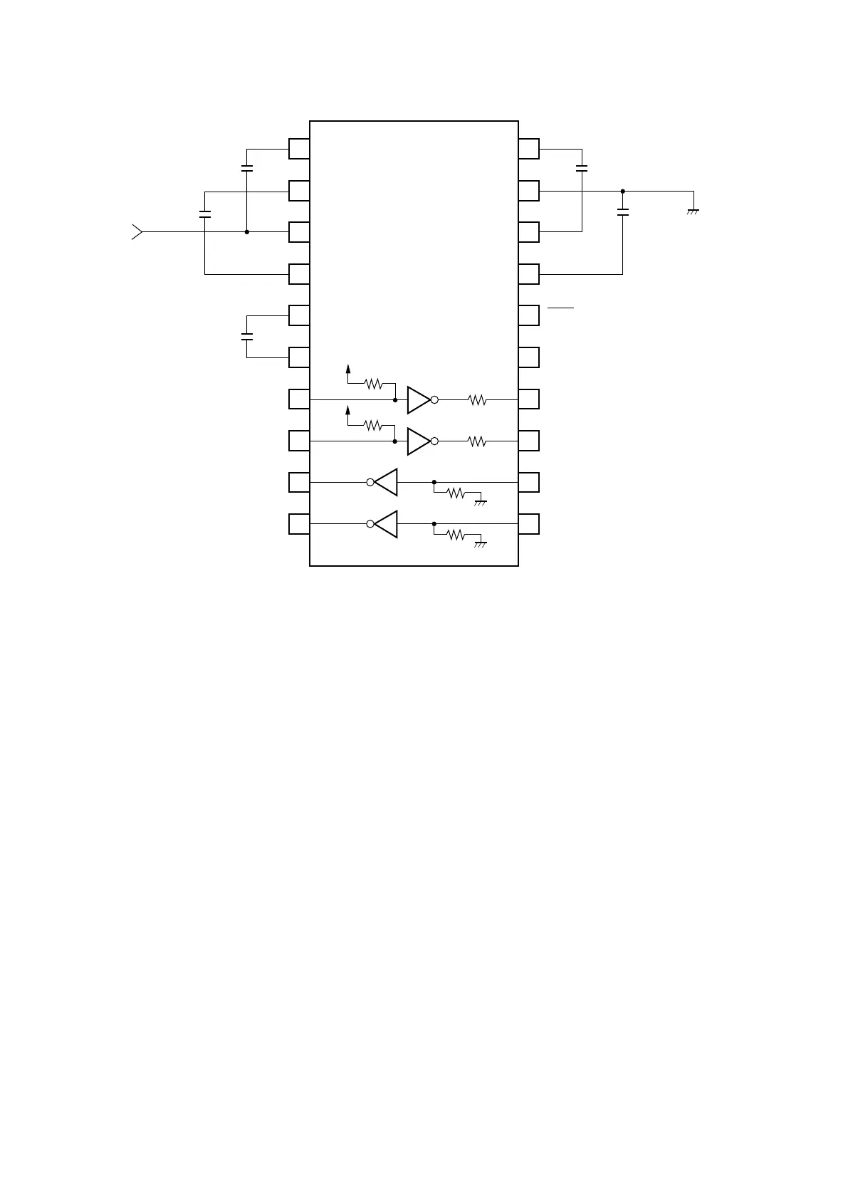
BLOCK DIAGRAM/PIN CONFIGURATION (Top View)
Note 1. VDD and VSS are output pins stepped up internally. These pins should not be loaded directly.
2. Capacitors C1 to C5 with a breakdown voltage of 20 V or higher are recommended. And it is
recommended to insert the capacitor that is 0.1
µ
F to 1
µ
F between VCC and GND.
3. If V
CHA is kept low level (in 5 V mode), capacitor C5 is not necessary.
4. The pull-up resistors at driver input are active resistors.
1
2
3
4
5
6
7
8
9
10
20
19
18
17
16
15
14
13
12
11
D
IN1
DIN2
ROUT1
ROUT2
STBY
V
CHA
DOUT1
DOUT2
RIN1
RIN2
VDD
C1
+
V
CC
C1
–
C
5
+
C5
–
C
4
+
GND
C
4
–
V
SS
+10 V
C
3
C1
C5
–10 V
+
C
2
C4
+
+
+
Note 4
300 Ω
300 Ω
5.5 kΩ
5.5 kΩ
+3.3 V
or
+5 V
+
 Loading...