EasyManua.ls Logo

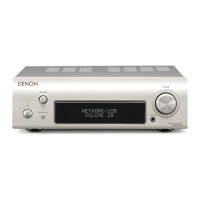
Denon DRA-F101 Service Manual

Denon DRA-F101
37 pages
To Next Page IconTo Next Page
Page #1 background imageLoading...
Page #1 background image
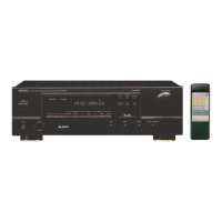
Hi-Fi AM-FM Stereo Receiver
SERVICE MANUAL
MODEL
DRA-F101
AM-FM STEREO RECEIVER
Some illustrations using in this service manual are slightly different from the actual set.
For Europe & U.K. model
16-11, YUSHIMA 3-CHOME, BUNKYOU-KU, TOKYO 113-0034 JAPAN
Telephone: 03 (3837) 5321
X0151 NC 0207

Other manuals for Denon DRA-F101

Questions and Answers:

Denon DRA-F101 Specifications

General IconGeneral
Number of Channels2
Frequency Response10 Hz - 100 kHz
Signal-to-Noise Ratio100 dB
Input sensitivity200 mV
Power consumption120 W
Total Harmonic Distortion (THD)0.1%
Input Impedance47k ohms
FM Tuning Range87.5 - 108 MHz
AM Tuning Range522 - 1611 kHz

Summary

Safety Precautions

Leakage Current Check

Safety check before unit return to customer.

Specifications

Power Amplifier Section

Rated output power and output terminals.

Pre Amplifier Section

Rated output, input sensitivity, impedance, RIAA deviation.

Overall Characteristics

SN ratio, frequency response, tone control range.

Tuner Section

Reception frequency, sensitivity, isolation, S/N, distortion.

Clock/Timer Section

Clock system, precision, timer functions.

Others

Power supply, consumption, dimensions, net mass.

Remote Control Unit (RC-927)

Remote system, power, dimensions, mass.

Disassembly Procedures

Top Cover Removal

Procedure to remove the top cover.

Front Panel Removal

Steps to remove the front panel assembly.

Display and Encoder PWB Removal

Detaching display and encoder boards.

System Connector PWB Removal

Removing the system connector circuit board.

Tuner Pack Removal

Procedure to disconnect and remove the tuner pack.

Power PWB and Heat Sink Removal

Removing the power board and heat sink.

Shield Plate, Back Panel, and Main PWB Removal

Removing shield plate, back panel, and main PWB.

Block and Level Diagram

Adjustment Procedures

Idling Current Adjustment

Procedure for setting and adjusting the idling current.

Check Procedures

Connection Diagram for Check

Diagram showing signal connections for testing.

Semiconductors

IC μPD780208GF-142-3BA Terminal Function

Pinout and function for the main IC.

FL Display Information

Grid Assignment

Layout and mapping of the FL display segments.

Pin Connection

Pinout description for the FL display connector.

Anode Connection

Anode connection mapping for display modes.

Printed Wiring Boards

Notes for Parts List

Parts List of PWB Unit Assembly

Semiconductors Group

List of semiconductor components on the PWB.

Resistors Group

List of resistors with part numbers and values.

Capacitors Group

List of capacitors with part numbers and specifications.

Other Parts Group

Exploded View

Parts List of Exploded View

DRA PWB Unit Parts

Components and assemblies for the DRA PWB.

Screws and Nuts

List of all screws and nuts used in assembly.

Packing View

Parts List of Packing & Accessories

List of packaging parts and accessories.

Wiring Diagram

Schematic Diagrams (Part 1)

1U-3458-1 Main Unit Schematic

Detailed schematic for the main control and processing unit.

1U-3458-5 System Control Unit Schematic

Schematic for the system control unit.

1U-3458-6 Power Amp Unit Schematic

Schematic for the power amplifier section.

Schematic Diagrams (Part 2)

1U-3458-2 Display Unit Schematic

Detailed schematic for the front panel display and control interface.

1U-3458-3 V. Encoder Unit Schematic

Schematic for the volume encoder unit.

1U-3458-4 F. Encoder Unit Schematic

Schematic for the function encoder unit.

Related product manuals