


W
watsonsaraJul 26, 2025
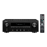
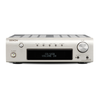
What to do if my Denon Receiver powers off with a blinking power LED?
- Kkimberly08Jul 26, 2025
If your Denon Receiver powers off and the power LED is blinking, check the power supply voltages for the analog block and the digital block.