1. IC's
R5F5631FDDFB (MAIN: IC20)
MAIN MCU PORT MAP
No. Port Name Function Name I/O Nor-
mal
STBY
OPT
STBY
Net-
work
STBY
Clock
display
mode
Detail of Function
1 AVSS0 AVSS - - - - - Ground Pin
2 P05/IRQ13 P_DOWN I I I I I Detect Power Down
3 VREFH VREFH - - - - - Reference Power Supply Pin
4 P03/IRQ11 DC_PROT1 I I I I I DC Protect1
5 VREFL VREFL - - - - - Connect to GND
6 P02/IRQ10/AN020 TOUCH_INT I I I I I Interrupt from Touch sensor IC.
7 P01/RXD6/IRQ9/AN019 reserved O O/L O/L O/L O/L NC (Open)
8 P00/TXD6/IRQ8/AN018 reserved O O/L O/L O/L O/L NC (Open)
9 PF5/IRQ4 SUB_PWR_CONT O O/L O/L O/L O/L On/Off control of SUB power
10 EMLE EMLE - - - - - E20 Emulator control pin (On chip Emulator is used,this pin
should be High. Not used,it should be Low)
11 PJ5 BURST_CONT O O/L O/L O/L O/L On/Off control of SMPS burst mode avoidance processing
12 VSS VSS - - - - - Ground Pin
13 PJ3 OPT_PWR_CONT O O/L O/H O/L O/L Opt-Jack Power On/Off control
14 VCL VCL - - - - - Smoothing Capacitor Connection Pin (0.1uF)
15 VBATT VBATT - - - - - Power supply pin
16 MD/FINED MD - - - - - Pins for setting the operating mode(select the Boot Mode or
User Boot Mode,Single Chip Mode)
17 XCIN XCIN - - - - - Pull Down
18 XCOUT XCOUT O O/L O/L O/L O/L NC (Open)
19 RES# RESET - - - - - Reset Signal Input Pin
20 XTAL/P37 XTAL - - - - - Pins for a crystal resonator (Xin=10MHzx10)
21 VSS VSS - - - - - Ground Pin
22 EXTAL/P36 EXTAL I - - - - Pins for a crystal resonator (Xin=10MHzx10)
23 VCC VCC - - - - - Power supply pin.
24 P35(IN)/NMI OPEN I I I I I OPEN (Input Only)
25 TRST#/P34/IRQ4 TRST# I I I I I E20 Emulator control pin/When normal operating mode,set to
input.
1
2
3
4
5
6
7
8
9
10
11
12
13
14
15
16
17
18
19
20
21
22
23
24
25
26
27
28
29
30
31
32
33
34
35
36
108
107
106
105
104
103
102
101
100
99
98
97
96
95
94
93
92
91
90
89
88
87
86
85
84
83
82
81
80
79
78
77
76
75
74
73
72
71
70
69
68
67
66
65
64
63
62
61
60
59
58
57
56
55
54
53
52
51
50
49
48
47
46
45
44
43
42
41
40
39
38
37
109
110
111
112
113
114
115
116
117
118
119
120
121
122
123
124
125
126
127
128
129
130
131
132
133
134
135
136
137
138
139
140
141
142
143
144
PE0
P64
P63
P62
P61
VSS
P60
VCC
PD7
PD6
PD5
PD4
PD2
PD1
PD0
P93
P92
P91
VSS
P90
VCC
P47
P46
P45
P44
P43
P42
P41
VREFL0
P40
VREFH0
P07
PE1
PD3
AVCC0
P74
PC2
P76
P77
PC3
PC4
P80
P81
P82
PC5
PC6
PC7
VCC
VSS
P50
P51
P52
P53
P54
P55
P56
VSS_USB
USB0_DP
USB0_DM
VCC_USB
P12
P13
P14
P15
P86
P16
P87
P20
P75
P83
P17
PE3
PE5
VSS
P70
VCC
PE6
PE7
P65
P66
P67
PA0
PA1
PA2
VSS
PA4
VCC
PA5
PA6
PA7
PB0
P71
P72
PB1
PB2
PB3
PB4
PB5
PB6
PB7
P73
VSS
PC0
PC1
PE4
PA3
VCC
AVSS0
VREFH
P03
VREFL
P02
P01
P00
PF5
EMLE
PJ5
VSS
PJ3
VCL
MD/FINED
XCIN
PH6/X COUT
RES#
P37/XTAL
VSS
P36/EXTAL
VCC
P35
P34
P32
P31
P30
P27
P26
P25
P24
P23
P21
P05
VBATT
P22
P33
PE2
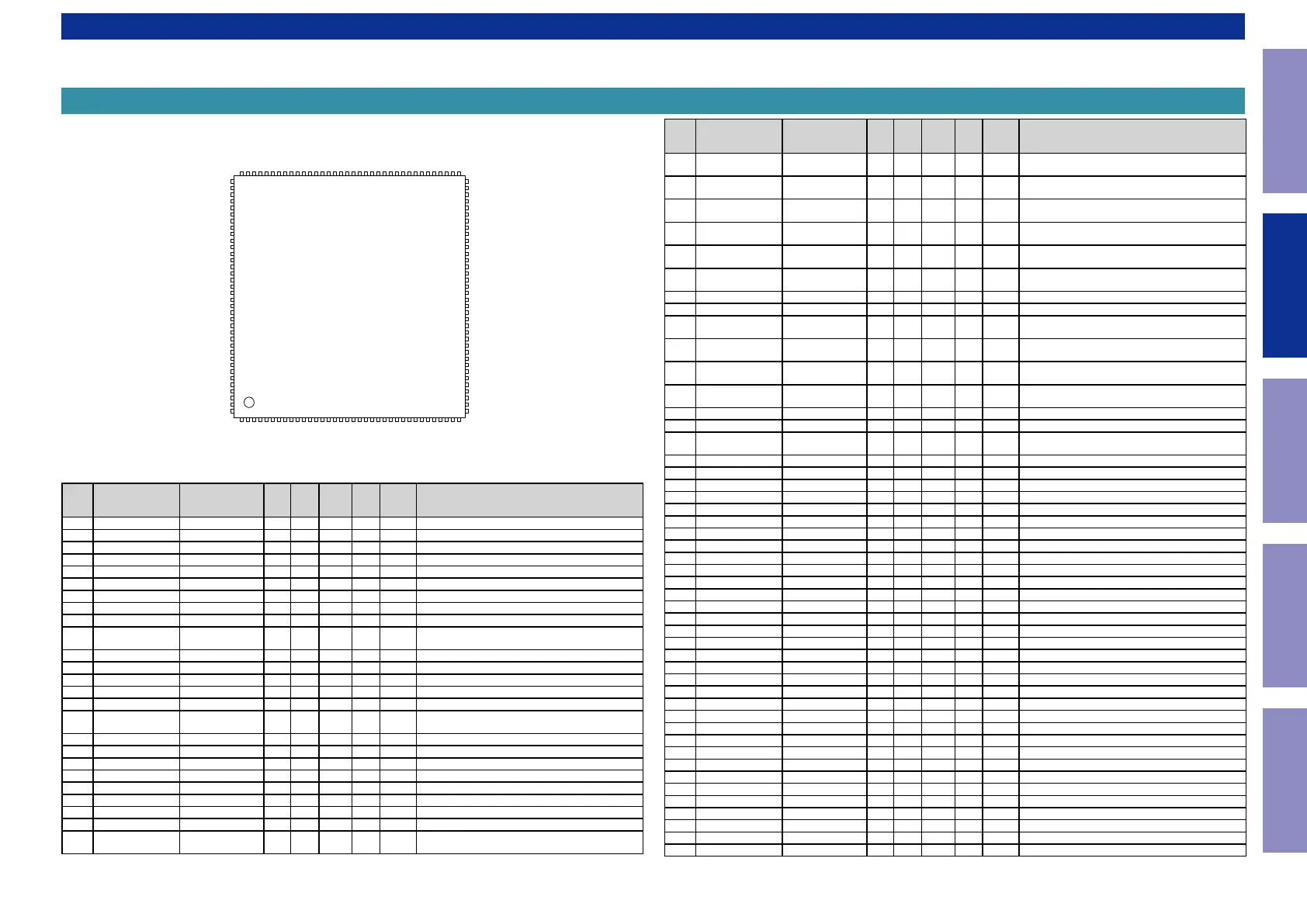
RX63N Group
RX631 Group
PLQP0144KA-A
(144-pin LQFP)
(Top view)
No. Port Name Function Name I/O Nor-
mal
STBY
OPT
STBY
Net-
work
STBY
Clock
display
mode
Detail of Function
26 P33/TIOCD0/RXD6/
RXD0/IRQ3-DS
REMOTE I I I I I Remote Input
27 P32/TXD6/TXD0/IRQ2-
DS
OLED_CONT O O/L O/L O/L O/H OLED Power Control Pin (3.3V)
28 TMS/P31/IRQ1-DS TMS I I I I I E20 Emulator control pin/When normal operating mode,set to
input.
29 TDI/P30/RXD1/IRQ0-DS TDI I I I I I E20 Emulator control pin/Mitsubishi writter control pin/When
normal operating mode,set to input.
30 TCK/FINEC/P27 TCK I I I I I E20 Emulator control pin//When normal operating mode,set to
input.
31 TDO/P26/TXD1 TDO O O/L O/L O/L O/L E20 Emulator control pin/Mitsubishi writter control pin/When
normal operating mode,set to input.
32 P25/RXD3 /A_SD I I I I I TAS5142 Shut-Down Detect
33 P24 /A_OTW I I I I I TAS5142 Over-Temperature Warning Detect
34 P23/TXD3 E_RTS_MOEI O O/L O/L O
(Com.)
O/L Ethernet (LEGO) Control Pin
35 P22/SCK0 E_CTS_MIEO I I I I
(Com.)
I Ethernet (LEGO) Control Pin
36 P21/RXD0/IRQ9 E_RXD_MIEO I I I I
(Com.)
I Ethernet (LEGO) Control Pin
37 P20/TXD0/IRQ8 E_TXD_MOEI O O/L O/L O
(Com.)
O/L Ethernet (LEGO) Control Pin
38 P17/TXD3/IRQ7 AIOS4_FACT_RST O O/H O/H O/H O/H Ethernet (LEGO) Control Pin *used by open drain port
39 P87 TU_RST O O/L O/L O/L O/L Tuner control
40 P16/TXD1/RXD3/IRQ6 NET5V_POWER O O/L O/L O/H O/L Ethernet Power Supply (NET5V) Control Pin, & +5V_CONT
Control Pin
41 P86 TU_SDA I/O I I I I Tuner control
42 P15/RXD1/IRQ5 TU_INT I I I I I Tuner control
43 P14/IRQ4 TU_SCL O O/L O/L O/L O/L Tuner control
44 P13/TXD2/IRQ3 TU_CE O O/L O/L O/L O/L Tuner control
45 P12/RXD2/IRQ2 S_FLASH_CLK O O/L O/L O/L O/L [E1C(CN) Region Model Only] GD25Q32-6P, CLK
46 VCC_USB VCC CPU - - - - - VCC (not 5VUSB)
47 USB0_DM reserved - - - - - NC (Open)
48 USB0_DP reserved - - - - - NC (Open)
49 VSS_USB VSS_USB - - - - - Ground pin
50 P56 S_FLASH_HOLD I/O I I I I [E1C(CN) Region Model Only] GD25Q32-7P,HOLD# ( IO3 )
51 P55/IRQ10 S_FLASH_WP I/O I I I I [E1C(CN) Region Model Only] GD25Q32-3P,WP# ( IO2 )
52 P54 S_FLASH_SO I/O I I I I [E1C(CN) Region Model Only] GD25Q32-2P,SO ( IO1 )
53 BCLK/P53 S_FLASH_SI I/O I I I I [E1C(CN) Region Model Only] GD25Q32-5P,SI ( IO0 )
54 P52/RXD2 S_FLASH_CS O O/L O/L O/L O/L [E1C(CN) Region Model Only] GD25Q32-1P, CS
55 P51/SCK2 DIR2_CLK O O/L O/L O/L O/L DIR PCM9211(Distribution) Control
56 P50/TXD2 DIR2_CE O O/L O/L O/L O/L DIR PCM9211(Distribution) Control
57 VSS VSS - - - - - Ground Pin
58 P83 SW_MUTE O O/L O/L O/L O/L Sub woofer output Mute
59 VCC VCC - - - - - Power Supply Pin.
60 PC7/TXD8/IRQ14 UB I I I I I Emulator Connection Pin
61 PC6/RXD8/IRQ13 DIR2_INT0 I I I I I DIR PCM9211(Distribution) Control
62 PC5 DC_PROT2 I I I I I DC Protect2
63 P82/TXD10 (DIR2_RERR) reserved O O/L O/L O/L O/L (DIR PCM9211(Distribution) Control) NC (Open)
64 P81/RXD10 /DIR2_RST O I I I I DIR PCM9211(Distribution) Control
65 P80/SCK10 DIR2_DO I I I I I DIR PCM9211(Distribution) Control
66 PC4 DIR2_DI O O/L O/L O/L
O/L DIR PCM9211(Distribution) Control
67 PC3/TXD5 /A_58_PDN O O/L O/L O/L O/L TAS5558 Power Down Port Control
68 P77/TXD11 /A_58_RESET O O/L O/L O/L O/L TAS5558 Reset Port Control
69 P76/RXD11 /HP_ON O O/L O/L O/L O/L TAS5558 SPK or Headphone Out Switch Control
70 PC2/RXD5 /A_58_MUTE O O/L O/L O/L O/L TAS5558 Mute Port Control
71 P75 /HP_MUTE O O/L O/L O/L O/L Headphone Mute Control
72 P74 (IOEXP_SDA) reserved I/O O/L O/L O/L O/L (I/O Expander I2C SDA) NC (Open)
73 PC1 (IOEXP_SCL) reserved O O/L O/L O/L O/L I/O Expander I2C SCL) NC (Open)
SEMICONDUCTORS
Only major semiconductors are shown, general semiconductors etc. are omitted to list.
The semiconductor which described a detailed drawing in a schematic diagram are omitted to list.
Before Servicing
This Unit
Electrical Mechanical Repair Information Updating
24
 Loading...