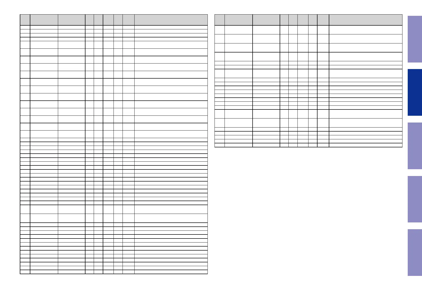
No. Port Name Function Name I/O Nor-
mal
STBY
OPT
STBY
Net-
work
STBY
Clock
display
mode
Detail of Function
74 VCC VCC - - - - - Power Supply Pin
75 PC0 (IOEXP_INT) reserved I O/L O/L O/L O/L (I/O Expander INT) NC (Open)
76 VSS VSS - - - - - Ground pin
77 P73 OLED_P_CONT O O/L O/L O/L O/H OLED Power Control Pin (16V)
78 PB7/TXD9 D7 O O/L O/L O/L O/H
(Com.)
Data bus for OLED
79 PB6/RXD9 D6 O O/L O/L O/L O/H
(Com.)
Data bus for OLED
80 PB5 D5 O O/L O/L O/L O/H
(Com.)
Data bus for OLED
81 PB4 D4 O O/L O/L O/L O/H
(Com.)
Data bus for OLED
82 PB3 D3 O O/L O/L O/L O/H
(Com.)
Data bus for OLED
83 PB2 D2 O O/L O/L O/L O/H
(Com.)
Data bus for OLED
84 PB1/TXD4/TXD6 D1 O O/L O/L O/L O/H
(Com.)
Data bus for OLED
85 P72 EL_CS O O/L O/L O/L O/H
(Com.)
If logic level "L", Enable communication with OLED.
86 P71 EL_RST O O/L O/L O/L O/H
(Com.)
OLED Reset Pin. Logic Level "L"=RESET
87 PB0/RXD4/RXD6/IRQ12 D0 O O/L O/L O/L O/H
(Com.)
Data bus for OLED
88 PA7 EL_DC O O/L O/L O/L O/H
(Com.)
OLED Data/Commando Switch. "H"=Data, "L"=Command
89 PA6 EL_RD O O/L O/L O/L O/H
(Com.)
OLED EL Read
90 PA5 EL_WR O O/L O/L O/L O/H
(Com.)
OLED EL Write
91 VCC VCC - - - - - Power Supply Pin
92 PA4/TXD5/IRQ5-DS SP_PROT I I I I I Speaker DC Voltage Protector Detection
93 VSS VSS - - - - - Ground Pin
94 PA3/RXD5/IRQ6-DS DIR_DI O O/L O/L O/L O/L DIR PCM9211(Main stream) Control
95 PA2/RXD5 DIR_DO I I I I I DIR PCM9211(Main stream) Control
96 PA1/MTIOC0B/IRQ11 DIR_CE O O/L O/L O/L O/L DIR PCM9211(Main stream) Control
97 PA0 DIR_CLK O O/L O/L O/L O/L DIR PCM9211(Main stream) Control
98 P67/IRQ15 DIR_INT0 I I I I I DIR PCM9211(Main stream) Control
99 P66 /DIR_RST O O/L O/L O/L O/L DIR PCM9211(Main stream) Control
100 P65 DIR_NPCM I I I I I DIR PCM9211(Main stream) Control
101 PE7/IRQ7/AN5 OPT1_DET I I I I I OPT1 Signal Input Detection
102 PE6/IRQ6/AN4 OPT2_DET I I I I I OPT2 Signal Input Detection
103 VCC VCC - - - - - Power Supply Pin
104 P70 /5100RST O O/L O/L O/L O/L DAC PCM5100 Reset & Mute Control
105 VSS VSS - - - - - Ground Pin
106 PE5/IRQ5/AN3 /A_58_SDA I/O I I I I TAS5558, NJU7251A, Touch Sensor I2C SDA
107 PE4/AN2 /A_58_SCL O I I I I TAS5558, NJU7251A, Touch Sensor I2C SCL
108 PE3 AIOS4_WAKEUP O O/L O/L O/H O/L Ethernet(LEGO) control pin for Standby(High:Normal,Low:Deep
Standby)
109 PE2/RXD12/IRQ7-DS/
AN0
AIOS4_STBY_STATUS I I I I I Status pin for UART communication with LEGO(L:not-available,
H:available)
110 PE1/TXD12 5100DEEMP O O/L O/L O/L O/L DAC PCM5100A De-Emphasis Control
111 PE0 NET3V3_POWER O O/L O/L O/H O/L "NET3.3V" Power Supply Control
112 P64 CD_INSW I I I I I CD Drive Limit SW Input
113 P63 CD_OPSW I I I I I CD Drive Opne SW Input
114 P62
CD_CLSW I I I I I CD Drive Close SW Input
115 P61 CD_DREQ I I I I I CD DSP DREQ Input (Input Only, Schmitt Trigger Input)
116 VSS VSS - - - - - Ground Pin
117 P60 CD_SBSY I I I I I CD Monitor 3 (default : Output)
118 VCC VCC - - - - - Power Supply Pin
119 PD7/IRQ7/AN7 CD_DECRST O O/L O/L O/L O/L CD DSP Reset
120 PD6/IRQ6/AN6 CD_BUCK O O/L O/L O/L O/L CD DSP Control : BUS CLK signal
121 PD5/IRQ5/AN013 CD_CCE O O/L O/L O/L O/L CD DSP Control : Chip Enable Signal
122 PD4/IRQ4/AN012 CD_SRAMSTB O O/L O/L O/L O/L CD DSP SRAMSTB control pin
No. Port Name Function Name I/O Nor-
mal
STBY
OPT
STBY
Net-
work
STBY
Clock
display
mode
Detail of Function
123 PD3/IRQ3/AN011 CD_BUS3 I/O O/L O/L O/L O/L CD DSP Control Pin (Need to connect the consecutive ports of
uCOM.)
124 PD2/IRQ2/AN010 CD_BUS2 I/O O/L O/L O/L O/L CD DSP Control Pin (Need to connect the consecutive ports of
uCOM.)
125 PD1/IRQ1/AN009 CD_BUS1 I/O O/L O/L O/L O/L CD DSP Control Pin (Need to connect the consecutive ports of
uCOM.)
126 PD0/TIOCA7/IRQ0/
AN008
CD_BUS0 I/O O/L O/L O/L O/L CD DSP Control Pin (Need to connect the consecutive ports of
uCOM.)
127 P93/AN017 CD_OPEN O O/L O/L O/L O/L CD Tray Open Control
128 P92/RXD7/AN016 CD_CLOSE O O/L O/L O/L O/L CD Tray Close Control
129 P91/AN015 CD_M_STBY O O/L O/L O/L O/L CD Driver Mute Off : "H"(Operating), Mute On : "L"(Non
Operating)
130 VSS VSS - - - - - Ground Pin
131 P90/TXD7/AN014 CD_LDCHK I I I I I CD Laser Diode Current Check. (Input to Analog Port)
132 VCC VCC - - - - - Power Supply Pin
133 P47/IRQ15-DS/AN007 LED_R O O/L O/L O/L O/L Front Red LED Control (NET STBY : Red)
134 P46/IRQ14-DS/AN006 LED Orange O O/L O/L O/L O/L Front Red&Green LED Control
135 P45/IRQ13-DS/AN005 HP_DET I I I I I H/P Plug Insert Detection
136 P44/IRQ12-DS/AN004 REGION I I I I I Region Discrimination Input (E2:3.3V, JP:2.27V, E1C:1.65V, E3:0V)
137 P43/IRQ11-DS/AN003 reserved O O/L O/L O/L O/L NC (Open)
138 P42/IRQ10-DS/AN002 KEY2 I I I I I EJECT Key Control Signal Input Pin (When standby mode, set to
inturrupt)
139 P41/IRQ9-DS/AN001 KEY1 I I I I I POWER Key Control Signal Input Pin (When standby mode, set
to inturrupt)
140 VREFL0 VREFL0 - - - - - Ground Pin
141 P40/IRQ8-DS/AN000 LED W O O/L O/L O/L O/H Front White LED Control
142 VREFH0 VREFH0 - - - - - Power Supply Pin
143 AVCC0 AVCC0 - - - - - Power Supply Pin
144 P07/IRQ15 LED_W_EJECT O O/L O/L O/L O/L Front Eject LED Control
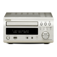
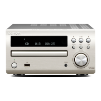
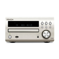
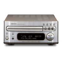
Before Servicing
This Unit
Electrical Mechanical Repair Information Updating
25
 Loading...