TAS5558 (MAIN: IC40)
TAS5558 Pin Discriptions
PWM_HPM_L
1
2
3
4
5
6
7
PWM_HPP_R
AVSS
PLL_FLTM
PLL_FLTP
SDIN1
VR_ANA
SDIN2
AVDD
ASEL_EMO2
SCLK
SDIN2_1
MCLK
OSCRES
DVSS2_CORE
EMO1
RESET
HP_SEL
PDN
MUTE
VR_DIG
LRCLK
SDA
SCL
PWM_HPP_L
PWM_HPM_R
8
9
10
11
12
13
14
15
16
17
18
19
20
21
22
23
24
25
26
27
28 29
30
31
32
33
34
35
36
37
38
39
40
41
42
43
44
45
46
47
48
49
50
51
52
53
54
55
56
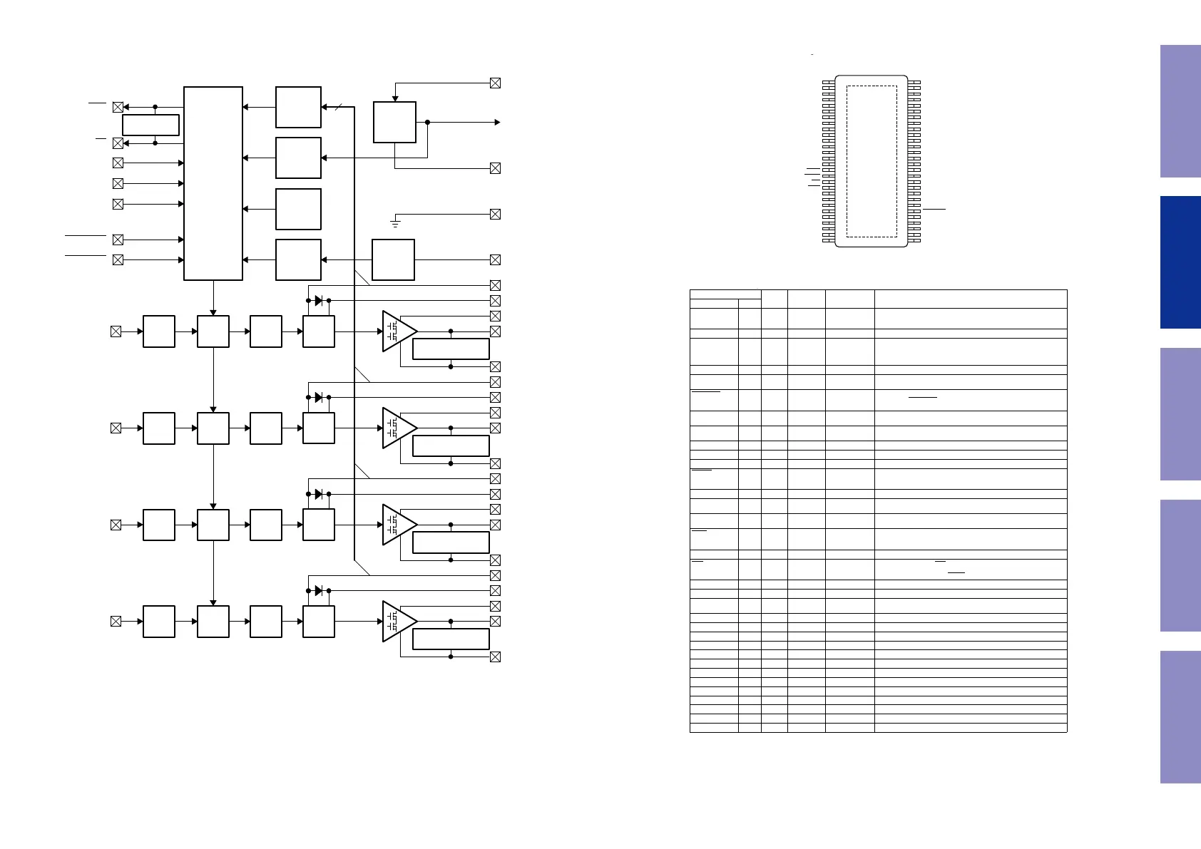
(Top View)
PWM_P_6
PWM_M_6
PWM_P_5
PWM_M_5
VR_PWM
AVSS_PWM
AVDD_PWM
PWM_P_8
PWM_M_8
PWM_P_7
PWM_M_7
PWM_P_4
PWM_M_4
PWM_P_3
PWM_M_3
PWM_P_2
PWM_M_2
PWM_P_1
VALID
DVDD1_CORE
PWM_M_1
DVSS1_CORE
BKND_ERR
PSVC/MLCK
TEST
SCLKO (SCLK_2)
SDOUT (SDIN5)
SDIN2_2
TAS5558
TAS5558
SLES273A –APRIL 2013 –REVISED JUNE 2013
www.ti.com
2 Device Information
2.1 Physical Characteristics
2.1.1 TAS5558 Pin Assignments
Figure 2-1. TAS5558 Pinout
4 Device Information Copyright © 2013, Texas Instruments Incorporated
Submit Documentation Feedback
Product Folder Links: TAS5558
TAS5558
www.ti.com
SLES273A –APRIL 2013–REVISED JUNE 2013
2.1.2 Pin Descriptions
PIN
5-V
TYPE
(1)
TERMINATION
(2)
DESCRIPTION
TOLERANT
NAME NO.
ASEL_EMO2 10 DIO Pullup I2C Address Select. Address will 0X34/0X36 with the value of pin being "0' or
"1" during de-assertion of reset. Can be programmed to be an output (as energy
manager output for subwoofer)
AVDD 9 P Analog supply (3.3 V) for PLL.
AVDD_PWM 50 P 3.3-V analog power supply for PWM. This terminal can be connected to the
same power source used to drive power terminal DVDD; but to achieve low PLL
jitter, this terminal should be bypassed to AVSS_PWM with a 0.1-μF low-ESR
capacitor.
AVSS 5 P Analog ground
AVSS_PWM 51 P Analog ground for PWM. Must have direct return Cu path to analog 3.3V supply
for optimized performance.
BKND_ERR 34 DI Pullup Active-low. A back-end error sequence is generated by applying logic low to this
terminal. The BKND_ERR results in no change to I2C parameters, with all H-
bridge drive signals going to a hard-mute state (Non PWM Switching).
DVDD1 35 P 3.3-V digital power supply. (It is recommended that decoupling capacitors of
0.1 μF and 10 μF be mounted close to this pin).
DVDD2 14 P 3.3-V digital power supply for PWM. (It is recommended that decoupling
capacitors of 0.1 μF and 10 μF be mounted close to this pin).
DVSS1 36 P Digital ground 1
DVSS2 13 P Digital ground 2
EMO1 15 DO Energy Manger Output interrupt - Asserted high when threshold is exceeded.
HP_SEL 17 DI 5 V Pullup Headphone/speaker selector. When a logic low is applied, the headphone is
selected (speakers are off). When a logic high is applied, speakers are selected
(headphone is off).
LRCLK 22 DI 5 V Pulldown Serial-audio data left/right clock (sampling-rate clock)
LRCLKO / 31 DIO 5V Pulldown LRCLK for I2S OUT. Can also be used as LRCKIN_2 (I2S Input for SDIN2_x
LRCKIN_2 and SRC Bank 2)
MLCK 11 DI 3.3-V master clock input. The input frequency of this clock can range from 2
MHz to 50 MHz.
MUTE 19 DI 5 V Pullup Soft mute of outputs, active-low (muted signal = a logic low, normal operation =
a logic high). The mute control provides a noiseless volume ramp to silence.
Releasing mute provides a noiseless ramp to previous volume.
OSCRES 12 DO 1MΩ Resistor Oscillator resistor (1% tolerance).
PDN 18 DI 5 V Pullup Power down, active-low.
PDN powers down all logic and stops all clocks
whenever a logic low is applied. The I2C parameters are preserved through a
power-down cycle, as long as RESET is not active.
PLL_FLTM 6 AIO PLL negative filter.
PLL_FLTP 7 AIO PLL positive filter.
PSVC/MCLKO 33 DO Power-supply volume control PWM output or MCKO for external ADC (SDIN5
Source)
PWM_HPM_L 1 DO PWM left-channel headphone (differential –)
PWM_HPM_R 3 DO PWM right-channel headphone (differential –)
PWM_HPP_L 2 DO PWM left-channel headphone (differential +)
PWM_HPP_R 4 DO PWM right-channel headphone (differential +)
PWM_M_1 38 DO PWM 1 output (differential –)
PWM_M_2 40 DO PWM 2 output (differential –)
PWM_M_3 42 DO PWM 3 output (differential –)
PWM_M_4 44 DO PWM 4 output (differential –)
PWM_M_5 53 DO PWM 5 output (lineout L) (differential –)
PWM_M_6 55 DO PWM 6 output (lineout R) (differential –)
PWM_M_7 46 DO PWM 7 output (differential –)
PWM_M_8 48 DO PWM 8 output (differential –)
PWM_P_1 39 DO PWM 1 output (differential +)
(1) Type: A = analog; D = 3.3-V digital; P = power/ground/decoupling; I = input; O = output
(2) All pullups are 20-μA weak pullups and all pulldowns are 20-μA weak pulldowns. The pullups and pulldowns are included to ensure
proper input logic levels if the terminals are left unconnected (pullups → logic-1 input; pulldowns → logic-0 input). Devices that drive
inputs with pullups must be able to sink 20 μA while maintaining a logic-0 drive level. Devices that drive inputs with pulldowns must be
able to source 20 μA while maintaining a logic-1 drive level.
Copyright © 2013, Texas Instruments Incorporated Device Information 5
Submit Documentation Feedback
Product Folder Links: TAS5558
TAS5142 Block Diagram
Temp.
Sense
M1
M2
RESET_AB
SD
OTW
AGND
OC_ADJ
VREG VREG
M3
Power
On
Reset
Under-
voltage
Protection
GND
PWM_D OUT_D
GND_D
PVDD_D
BST_D
Timing
Gate
Drive
PWM
Rcv.
Overload
Protection
I
sense
GVDD_D
RESET_CD
4
Protection
and
I/O Logic
PWM_C OUT_C
GND_C
PVDD_C
BST_C
Timing
Gate
Drive
Ctrl.
PWM
Rcv.
GVDD_C
PWM_B OUT_B
GND_B
PVDD_B
BST_B
Timing
Gate
Drive
Ctrl.
PWM
Rcv.
GVDD_B
PWM_A OUT_A
GND_A
PVDD_A
BST_A
Timing
Gate
Drive
Ctrl.
PWM
Rcv.
GVDD_A
Ctrl.
BTL/PBTL−Configuration
Pulldown Resistor
BTL/PBTL−Configuration
Pulldown Resistor
BTL/PBTL−Configuration
Pulldown Resistor
BTL/PBTL−Configuration
Pulldown Resistor
Internal Pullup
Resistors to VREG
TAS5142
SLES126B–DECEMBER 2004 – REVISED MAY 2005
7
Before Servicing
This Unit
Electrical Mechanical Repair Information Updating
32
 Loading...