ICE3BS03LJG (SMPS: IC91)
ICE3BS03LJG Pin Discriptions
Pin Symbol Function
1 BL extended Blanking and Latch off enable
2 FB Feedback
3 CS Current Sense
4 Gate Gate driver output
5 HV High Voltage input
6 NC Not connected
7 VCC Controller Supply Voltage
8 GND Controller Ground
(1) at Tj=110C°
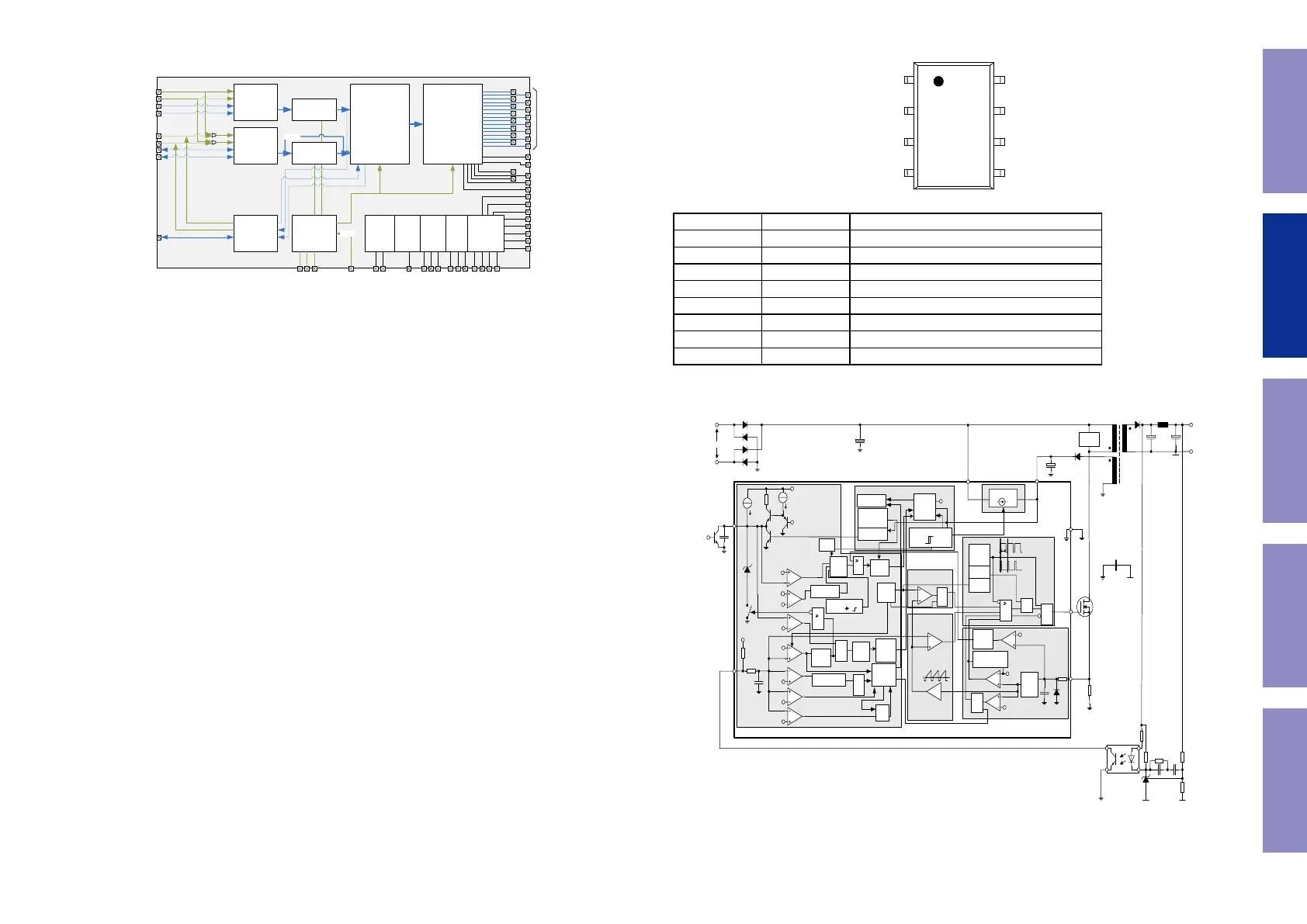
ICE3BS03LJG Block Diagram
Version 2.0 5 6 Dec 2007
F3 PWM controller
ICE3BS03LJG
Pin Configuration and Functionality
1 Pin Configuration and Functionality
1.1 Pin Configuration with PG-DSO-8
Figure 1 Pin Configuration PG-DSO-8(top view)
1.2 Pin Functionality
BL (extended Blanking and Latch off enable)
The BL pin combines the functions of extendable
blanking time for entering the Auto Restart Protection
Mode and the external latch off enable. The extendable
blanking time function is to extend the built-in 20ms
blanking time by adding an external capacitor at BL to
ground. The external latch off enable function is an
external access to latch off the IC. It is triggered by
pulling down the BL pin to less than 0.25V.
FB (Feedback)
The information about the regulation is provided by the
FB Pin to the internal Protection Unit and to the internal
PWM-Comparator to control the duty cycle. The FB-
Signal is the only control in case of light load at the
Active Burst Mode.
CS (Current Sense)
The Current Sense pin senses the voltage developed
on the series resistor inserted in the source of the
Power MOSFET. If CS reaches the internal threshold
of the Current Limit Comparator, the Driver output is
immediately switched off. Furthermore, this current
information can be used to realize the Current Mode
operation through the PWM-Comparator where it
compares with FB signal.
Gate
The Gate pin is the output of the internal driver stage
connected to the Gate of an external power MOSFET.
HV (High Voltage)
The high voltage Pin is connected to the rectified DC
input voltage. It is the input for the integrated 500V
Startup cell.
VCC (Power supply)
The VCC pin is the positive supply of the IC. The
operating range is between 10.5V and 26V.
GND (Ground)
The GND pin is the ground of the controller.
Pin Symbol Function
1 BL extended Blanking and Latch off
enable
2 FB Feedback
3 CS Current Sense
4 Gate Gate driver output
5 HV High Voltage input
6 n.c. Not Connected
7 VCC Controller Supply Voltage
8 GND Controller Ground
Package PG-DSO-8
1
6
7
8
4
3
2
5
GNDBL
FB
CS
VCC
N.C.
Gate
HV
Version 2.0 6 6 Dec 2007
F3 PWM controller
ICE3BS03LJG
Representative Blockdiagram
Internal Bias
Volt age
Reference
Oscill ator
Duty Cycle
max
x3.2
Current Limiting
PWM OP
Current Mode
Soft Start
C2
25.5V
R
FB
Power Management
C
BK
C
VCC
85 ... 270 VAC
C
Bulk
+
Converter
DC Output
V
OUT
PWM
Comparator
C3
4.0V
C4
4.0V
Gat e
Dri ver
0.72
Clock
R
Sense
10kΩ
D1
C6a
3.0V
C5
1.23V
C10
R
S
Q
Auto
Restart
Mode
&
G7
&
G5
&
G9
1
G8
0.9V
S1
1
Power-Down
Reset
CS
BL
GND
C7
C8
FB
PWM
Secti on
Control Unit
FF1
C12
&
0.25V
Leading
Edge
Blanking
220ns
25kΩ
2pF
5.0V
G10
1pF
Propagat ion-Delay
Compensation
5.0V
Undervol tage Lockout
V
csth
G2
-
ICE3XS03LJ-F3 PWM controller ( Latch and Jitter Mode )
Snubber
VCC
Startup Cell
C6b
&
G6
3.5V
&
G11
Active Burst
Mode
0.6V
10.5V
18V
#1
# : optional external components;
#1 : C
BK
is used to extend the Blanking Time
#2 : T
AE
is used to enable the external Latch off feature
Freq. jitter
20ms
Blanking
Ti me
20ms Blanki ng
Ti me
120us
Blanking Ti me
Soft
Start
Block
Soft-Start
Comparator
Spike
Blanki ng
30us
T2
3.25kΩ
5.0V
T1
T3 0.6V
I
BK
VCC
Latch off
Enable
Signal
T
AE
C9
0.25V
#2
C11
1.66V
Spike
Blanking
190ns
Latched off
Mode Reset
V
VCC
< 6.23V
Spike
Blanki ng
30us
G3
Latch off
Mode
Thermal Shutdown
T
j
>130°C
1
HV
Gat e
1 ms
counter
2 Representative Blockdiagram
Figure 2 Representative Blockdiagram
TAS5558 Block Diagram
Serial Audio
Receiver
2x Stereo
Serial Audio
Receiver
2x Stereo
Serial Audio
Transciever
Stereo
4ch ASRC
4ch ASRC
Fixed Flow
Digital Audio
Processor
(DAP)
10ch input
8ch Processor
8ch Output Mixer
Clocks
(Osc, PLL
etc)
12.288
8ch PWM
Generator
+ Headphone
(PWM)
Bypass
MCU
I2C
Control
Power
Supply
Volume
Control
(PSVC)
Energy
Manager
(EMO)
Power
SDA
SCL
SDOUT/SDIN5
SDIN1
SDIN2
SCLK
LRCLK
SDIN2-1
SDIN2-2
SCLKO /SCLKIN_2
OSCRES
PLL_FLTM
PLL_FLTP
MCLK
EMO1
ASEL_EMO2
VR_DIG
VR_PWM
VR_ANA
AVDD
AVDD_PWM
AVSS
AVSS_PWM
DVDD1
DVDD2
DVSS1
DVSS2
/PDN
/BKND_ERR
PWM_x_1
through 8
ASEL_EMO2
VALID
/MUTE
TEST
RESET
/HP_SEL
TAS5558
www.ti.com
SLES273A –APRIL 2013 – REVISED JUNE 2013
These devices have limited built-in ESD protection. The leads should be shorted together or the device placed in conductive foam
during storage or handling to prevent electrostatic damage to the MOS gates.
1.4 Block Diagram
Figure 1-1. Functional Block Diagram
1.5 DESCRIPTION (Continued)
The TAS5558 can drive eight channels of H-bridge power stages. Texas Instruments Power Stages are
designed to work seamlessly with the TAS5558. The TAS5558 supports either the single-ended or bridge-
tied-load configuration. The TAS5558 also provides a high-performance, differential output to drive an
external, differential-input, analog headphone amplifier.
The TAS5558 supports AD, BD, and ternary modulation operating at a 384-kHz switching rate for 48-, 96-,
and 192-kHz data. The 8× oversampling combined with the fourth-order noise shaper provides a broad,
flat noise floor and excellent dynamic range from 20 Hz to 32 kHz.
TAS5558 also features power-supply-volume-control (PSVC) improves dynamic range at lower power
level and can be used as part of a Class G Power Supply when used with closed loop PWM input power
stages.
Copyright © 2013, Texas Instruments Incorporated Device Information 3
Submit Documentation Feedback
Product Folder Links: TAS5558
Before Servicing
This Unit
Electrical Mechanical Repair Information Updating
33
 Loading...