TC390_MLF32(Touch sensor: U1)
Pin Conguration
Pin Description
32
31 30 29
28 27
26 25
9
10
11 12 13 14 15
16
1
2
3
4
5
6
7
8
24
23
22
21
20
19
18
17
TouchCore390
-ML32IP
VSS
(Bottom PAD)
VDDIO
RXD / SSB / I2C1_SDA / INT0 / T0 / P3.0
TXD / SCLK / I2C1_SCL / INT1 / T1 / P3.1
MISO / INT2 / P3.2 / RESETB
VDDINT
MOSI / I2C0_SDA / XTAL2 / INT3 / P3.3
I2C0_SCL / XTAL1 / INT4 / P3.4
VDDINTTS
P1.7 / TS1.7 / ADC1.7
P1.6 / TS1.6 / ADC1.6
P1.5 / TS1.5 / ADC1.5
P1.4 / TS1.4 / ADC1.4
P1.3 / TS1.3 / PWM1.3 / ADC1.3
P1.2 / TS1.2 / PWM1.2 / ADC1.2
P1.1 / TS1.1 / PWM1.1 / ADC1.1
P1.0 / TS1.0 / PWM1.0 / ADC1.0
P2.7 / TS2.7 / ADC2.7
P2.6 / TS2.6 / ADC2.6
P2.5 / TS2.5 / ADC2.5
P2.4 / TS2.4 / ADC2.4 / T2
P2.3 / TS2.3 / ADC2.3
P2.2 / TS2.2 / ADC2.2
P2.1 / TS2.1 / ADC2.1
P2.0 / TS2.0 / ADC2.0
ADC0.0 / PWM0.0 / P0.0
ADC0.1 / PWM0.1 / P0.1
ADC0.2 / PWM0.2 / P0.2
ADC0.3 / PWM0.3 / P0.3
ADC0.4 / PWM0.4 / P0.4
ADC0.5 / PWM0.5 / P0.5
ADC0.6 / PWM0.6 / P0.6
ADC0.7 / PWM0.7 / P0.7
24-pin MLF Package Diagram
6 / 15
Pin No. Name Type Description Share Pins
1
RXD / SSB / I2C1_SDA / INT0 / T0
3
TXD / SCLK / I2C1_SCL / INT1 / T1
4
5
Digital Power Filter ( +1.8V )
INT3 / XTAL2 / I2C0_SDA / MOSI
7
8
Touch Sensor Power Filter
9
10
12
14
16
17
Touch Sensing Channel 1.0
18
Touch Sensing Channel 1.1
19
Touch Sensing Channel 1.2
20
Touch Sensing Channel 1.3
21
Touch Sensing Channel 1.4
Touch Sensing Channel 1.5
23
Touch Sensing Channel 1.6
Touch Sensing Channel 1.7
25
Touch Sensing Channel 2.0
Touch Sensing Channel 2.1
27
Touch Sensing Channel 2.2
28
Touch Sensing Channel 2.3
29
Touch Sensing Channel 2.4
30
Touch Sensing Channel 2.5
Touch Sensing Channel 2.6
32
Touch Sensing Channel 2.7
NR111E (SMPS: IC95)
NR111E Pin Discriptions
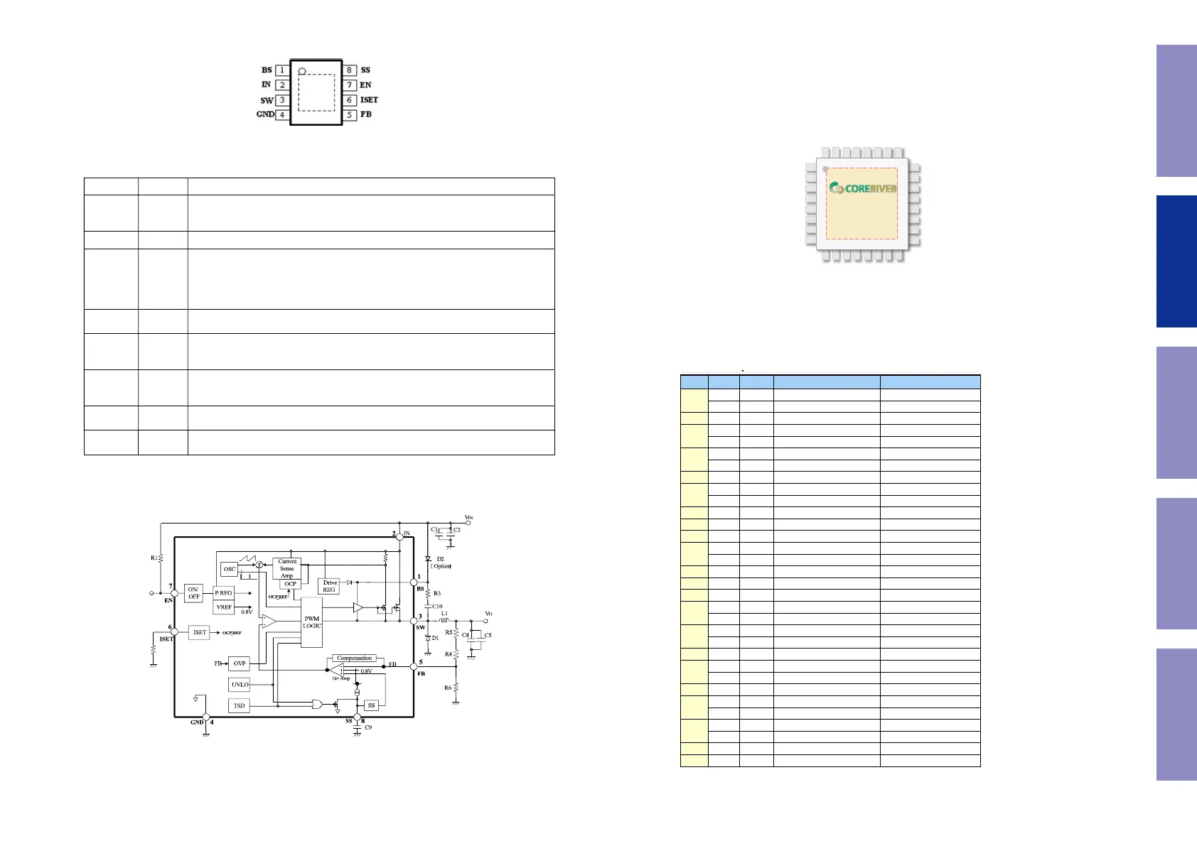
NR111E Block Diagram
Light Load High Efficiency, 31V, Buck Regulator
NR110E series
SANKEN ELECTRIC CO., LTD.
Oct/23/2012
Rev.1.0
6
http://www.sanken-ele.co.jp
Pin Assignments & Functions
Pin Assignments
Pin Functions
noitpircseD lobmyS .oN niP
1 BS
High-side Boost input.
BS supplies the drive for High-side Nch-MOSFET switch.
Connect a capacitor and a resistor between SW to BS.
2 IN
Power input. IN supplies the power to the IC as well as the regulator switches
3
SW
Power switching output.
SW supplies power to the output.
Connect the LC filter from SW to the output.
Note that a capacitor is required from SW to BS to supply the power the High-side
switch
4 GND
Ground
Connect the exposed pad to Pin No.4
5 FB
Feedback input Pin to compare Reference Voltage. The feedback threshold is 0.8V.
To set the output voltage, FB Pin is required to connect between resistive voltage
divider R4
and R6.
6 ISET
Adjust Pin of OCP starting current
OCP starting current can be adjusted by connecting a resistor to ISET Pin.
In the case of using at Maximum Io, ISET Pin is required to connect to GND.
7 EN
Enable input.
Drive EN Pin high to turn on the regulator, low to turn it off.
8 SS
Soft-Start control input.
To set the soft-start period, connect to a capacitor between GND.
Light Load High Efficiency, 31V, Buck Regulator
NR110E series
SANKEN ELECTRIC CO., LTD.
Oct/23/2012
Rev.1.0
6
http://www.sanken-ele.co.jp
Pin Assignments & Functions
Pin Assignments
Pin Functions
noitpircseD lobmyS .oN niP
1 BS
High-side Boost input.
BS supplies the drive for High-side Nch-MOSFET switch.
Connect a capacitor and a resistor between SW to BS.
2 IN
Power input. IN supplies the power to the IC as well as the regulator switches
3 SW
Power switching output.
SW supplies power to the output.
Connect the LC filter from SW to the output.
Note that a capacitor is required from SW to BS to supply the power the Hig
switch
4 GND
Ground
Connect the exposed pad to Pin No.4
5 FB
Feedback input Pin to compare Reference Voltage. The feedback threshold is 0.8V.
To set the output voltage, FB Pin is required to connect between resistive v
divider R4 and R6.
6 ISET
Adjust Pin of OCP starting current
OCP starting current can be adjusted by connecting a resistor to ISET Pin.
In the case of using at Maximum Io, ISET Pin is required to connect to GND.
7 EN
Enable input.
Drive EN Pin high to turn on the regulator, low to turn it off.
8 SS
Soft-Start control input.
To set the soft-start period, connect to a capacitor between GND.
Light Load High Efficiency, 31V, Buck Regulator
NR110E series
SANKEN ELECTRIC CO., LTD.
Oct/23/2012
Rev.1.0
6
http://www.sanken-ele.co.jp
Pin Assignments & Functions
Pin Assignments
Pin Functions
noitpircseD lobmyS .oN niP
1 BS
High-side Boost input.
BS supplies the drive for High-side Nch-MOSFET switch.
Connect a capacitor and a resistor between SW to BS.
2 IN
Power input. IN supplies the power to the IC as well as the regulator switches
3
SW
Power switching output.
SW supplies power to the output.
Connect the LC filter from SW to the output.
Note that a capacitor is required from SW to BS to supply the power the High-side
switch
4 GND
Ground
Connect the exposed pad to Pin No.4
5 FB
Feedback input Pin to compare Reference Voltage. The feedback threshold is 0.8V.
To set the output voltage, FB Pin is required to connect between resistive voltage
divider R4
and R6.
6 ISET
Adjust Pin of OCP starting current
OCP starting current can be adjusted by connecting a resistor to ISET Pin.
In the case of using at Maximum Io, ISET Pin is required to connect to GND.
7 EN
Enable input.
Drive EN Pin high to turn on the regulator, low to turn it off.
8 SS
Soft-Start control input.
To set the soft-start period, connect to a capacitor between GND.
Before Servicing
This Unit
Electrical Mechanical Repair Information Updating
34
 Loading...