EMC® VNX5300™ Hardware Information Guide
20
EMC® VNX5300™ Hardware Information Guide
Table 10 lists the SPS (RJ-12) pin signals used on the connector.
RJ-12 modular jack to micro DB-9 cable
The cable connecting the SPS to the SP is an RJ-12 to micro DB-9 cable (plug). It has an
RJ-12 connector (SPS side) on one end and a micro DB-9 connector (SP side) on the
other end. Figure 14 shows an example of an SPS A to SP A cable.
Figure 14 Example of SP A, MGMT A (micro DB-9) to SPS A (RJ-12) cable
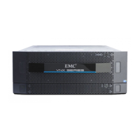
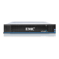
DPE rear view Figure 15 shows an example of a DPE with two SPs and the location of the major
hardware components that make up each SP (A and B).
Figure 15 Example of the Block and File VNX5300 platform DPE with two SPs (rear view)
Table 10 SPS (RJ-12) port and connector pinout
RJ-45 pin Signal Description
1 RTS/DSR Ready to send/Data transmit ready
2 Shield Shield
3 TXD Transmit data
4 RXD Receive data
5 GND Ground
6 CTS/DCD Clear to send/Data
VNX-000283
1 SP (for closer view, see Figure 16 on page 22) 3 I/O module slots showing one four-port 8-Gb/s
Fibre Channel (FC) I/O module (supports 2, 4,
and 8 Gb/s) and one four-port 1-Gb/s iSCSI I/O
module
2 Power supply (for closer view, see Figure 17 on
page 23)
4 CPU module (for closer view, see Figure 16 on
page 22)
X4
2
3
4
5
6Gb
SAS
8Gb
bre
1
0 X4
6Gb SAS
B
X4
2
3
4
5
6Gb
SAS
8Gb
bre
1
0 X4
6Gb SAS
A
Cover
Do not remove
Cover
Do not remove
Cover
Do not remove
Cover
Do not remove
4
SP B SP A
2
31
VNX-000287