CONFIDENTIAL
3 PCB Layout Design
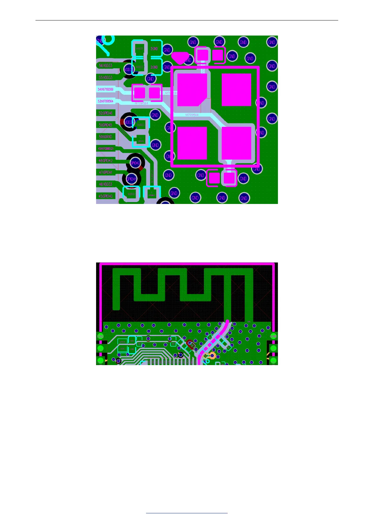
Figure 17: ESP32S3 Crystal Oscillator Layout
3.5 RF
The RF trace is routed as shown highlighted in pink in Figure 18.
Figure 18: ESP32S3 RF Layout in a Fourlayer PCB Design
• The RF trace should have 50 Ω single-ended characteristic impedance. The reference plane is the second
layer. A π-type matching circuit and an LC filter circuit should be added on the RF trace and placed close
to the chip, in a zigzag.
• For designing the RF trace at 50 Ω single-ended impedance, please refer to the PCB stack-up design
shown in Figure 19.
• The RF trace should have consistent width and not branch out. It should be as short as possible with
dense ground vias around for inteference shielding.
• The RF trace should be routed on the outer layer without vias, i.e., should not cross layers. The RF trace
should be routed at a 135° angle, or with circular arcs if trace bends are required.
Espressif Systems 22
Submit Documentation Feedback
ESP32-S3 Series Hardware Design Guidelines v1.0
 Loading...