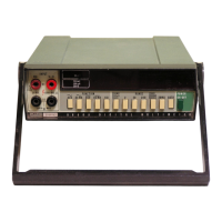
8600A
verter to the
input of the A/D Converter.
By inserting a
voltage at TP1
1 ,
all input signal conditioners
will
be
by-
passed.
The operation of the
A/D
Converter
and the
Control and
Display sections (with the exception
of the
range controls)
can
be checked
with the following
test.
If
the
instrument
passes this test, the
indication is that
the fault
is in the Input Divider
or in the range
selection.
a.
Select
the DCV function
and the
200mV range.
b.
With
no input to the Vf2
terminals,
check the
voltage
at
TP1
1 ,
and at buffer input
(U4 pin
3).
If
it is
OV proceed to the next
step.
A
voltage
on TP1
1 or at the buffer
input indicates that
one
of the
control FETs
(Q14, Q15, Q16, Q17, Q21)
or
Q13
or
Q1
1 may be shorted or
leaky.
c. Connect
+190mV to TP1
1 and
the
return lead to
TP3.
Refer
to table
4-10
and observe
the front
panel display
as the front panel range
switches are
changed.
RANGE
SETTING
DISPLAY
200 mV
+190.00
2V
+
.19
20V
+
1.90
200V
+
19.00
1200V
+190.00
AUTO
DECIMAL
MAY BE
ANYWHERE
REPEAT FOR NEGATIVE INPUT
Table
4-10
INPUT
DIVIDER
TEST
446.
OHMS
CONVERTER
447.
An instrument malfunction affecting
only the
ohms mode
of operation
is
generally the
result of the
ohms converter
producing an improper
level
of current
for
the particular resistance range being
used. The
follow-
ing
procedure
should be used to
evaluate
the operation
of
the ohms converter.
a.
Select the
Kfi
function
and
20
K range.
b. Place
a good quality short
across the V-S2
input
terminals.
c. Measure
the
voltage level at the
cathode of
CR2.
It
should be +10 ±0.1V
dc.
d. If
the voltage
is
incorrect
measure the voltage at
pin 3 of U
1 . This
point should
be 0.00 volts
+
100 microvolts.
e.
A
voltage
level greater
than ten volts at CR2
and
zero volts
at
pin
3 of U1 would indicate that
the
current
source
(Q3,
U3 and associated com-
ponents)
is supplying
more current than normal.
If the voltage
at
CR2 were less than ten volts
the current
from
Q3
would probably
be
less than
normal.
448. The operation of the current source
can
be
checked
by
measuring the voltage at
pins 2 and 3
of
U3.
The voltage on both
pins should be approximately
—8.6
volts. Uneven voltages
may be caused
by
improper re-
sistance value of
R35
or
R9
1 ,
or
a failure in CR1 0. The
voltages
at pin 2 and 3
of
U3 may be proper and
the
cur-
rent
supply
from
Q3
improper if
the gate of
Q3
were
leaking current back
to
pin 6 of U3.
449. CURRENT SHUNTS
4-50.
Failures in the current mode
of
operation affect-
ing all current ranges would probably be attributed
to a
failure
in
one of
the
following
areas:
1)
the input
fuse
(FI) open,
2)
one or more of diodes CR1, CR6, CR7,
or
CR8
shorted, or
3)
improper connection in the
con-
tacts of function switch S2 (ACI), or
S4
(DCI)
or range
switches S6-S10.
4-51.
AC
CONVERTER
4-52. Generally
a
failure
in the
ac
converter will do
one of two
things:
1)
create
a dc voltage output without
an ac input
signal applied to
the
8600A input
terminals
or
2)
not
produce the proper
dc
voltage
output
when
an
ac input is applied to the unit.
A dc
offset voltage created
within the ac converter
may cause
the
multimeter display
to indicate some substantial
value of
ac
voltage
when
a
short
is placed across the input terminals. When
the
ac
converter failure causes the display
to
remain at zero when
an ac signal is applied to the input,
the
converter is not
producing the proper dc voltage output for the A/D con-
verter.
4-53.
The operation of the
ac
converter
can
be checked
for the dc
voltage offset
by performing the
following pro-
cedure.
a.
Remove
the
molded
plastic
outer
case
from the
8600A (see
par.
4-7
Access/Dissassembly).
b.
Remove
the ac converter pcb,
take
the
metal
shield
off
the side and reinstall the board into
mainframe.
NOTE!
Take care that
all
the connector pins on the
board are properly aligned
before
seating the
pcb.
4-8
1/77