Q4,
Q5,
and
Q7
provide
the
necessary
voltage gain of
the
ac s:^nal.
Emitter-follower
0^
is the dynamic load
at
the amplifier output.
Feedback from the emitter of
Q7
through QlO
stabilizes the current and
voltage gain
of the amplifier. Transistors
Q2
and
Q9
provide a
low-
impedance bias voltage
for their associated
circuitry.
Linearity compensation at
the
d
3
mamic load oi±put is pro-
vided through
Q8.
Loop gain
of the
amplifier is
stabil-
ized
with the filters Cl, Rll and
C25, R44 selected
with
the
RANGE switch S9BR-2. The output
s^nal coupled
through C12 drives the
diodes CR3 and CR4
through their
cross-over
region very rapidly, thus
producing very low
cross-over distortion.
The signal develq)ed
across R125
is
fed
back to the
input of the AC Converter
through the
feedback network selected
with the RANGE switch
S9BR-1
and causes a
current directly
proportional to the ac
input
s%nal to flow
through CR3 and CR4.
The resulting dc
voltages are then filtered by
C13 and Cl4 and
applied
through the MODE switch S9 to
the
dc
measurement
section
of
the instrument. Calibration
of the ac voltage
ranges
of
the instrument is
accomplished with the
variable
resistors
R29, R30, R32, R34, variable
capacitors C21
and C22, and the
capacity compensator located
across
R12.
3-37.
The
3
kHz drive signal applied
between A7 ter-
minals 6 and
7
is
half-wave rectified
by
diodes CR5 and
CR6.
The resulting dc
voltages
are
then
reduced and
filtered with
R40, R4l, C23, and C24 to
provide the
±12
and
±10
volt dc pperattog vottages for
the
AC Converter.
3-38.
NULL
DETECTOR
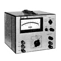
3-39. GENERAL. The Null Detector is a
chopper stabil-
ized
dc amplifier
usii^
an
insulated field effect transis-
tor as a chopper.
DC pperatii^ voltages for the
amplifier
are produced from a 3 kHz drive signal si?)plied
by the
dc-
to-dc converter, thus providing maximum isolation for
the amplifier circuitry free from power line frequency
variations and
harmonics. Circuitry
of the
Null Detector
consists of
a
power sxippiy, an 84 Hz multivibrator, a
chopper driver,
a
chopper, a low-pass filter,
a
carrier
amplifier,
a
synchronous demodulator and a meter. A
block diagram of these circuits is illustrated in
Figure
3-4.
3-40. BLCX:K diagram DESCRIPTION. AU
operating
voltages for the Null Detector circuitry are provided by
the power supply
comprised
of half-wave rectifiers
CR3
and
CR4. These ±6.
8
volt dc voltages are produced from
a 3 klfe drive
s%nal developed in the Reference Inverter.
The 84 Hz multivibrator provides chopper
and
demod-
ulator
drive voltages at
a
rate asjmchronous to the power
line
frequency. Input dc voltages applied to the null de-
tector u
5
)ufc are passed through a low-pass filter to
reduce
any normal mode
hriierference and then squarewave modu-
lated at
a
84 Hz rate by the
chopper
Ql,
The chopper
driver Qll
provides a 84 Hz drive signal to the gate
of
the chopper and a cancellation signal to
the
drain.
This
cancellation signal is
180°
out of
phase
with
the chopper
gate signal
and provides cancellation of any spikes gen-
erated internally
in the chopper
Ql.
The
carrier amp-
lifier is
conprised of five st^es
whose gain is controlled
by
negative emitter feedback.
Any amplified ac
annals
are
then demodulated
by
the synchronous
demodulator
Q8
which is driven in synchronism
with the chcpper
Ql.
The
resulting dc voltage is then used to drive the front
panel
meter to indicate
both the polarity and magnitude the
input voltage on the
TVM
mode or the off-null
magnihide
on
the
NULL
mode.
Negative feedback through the meter
to the null detector input determines the overall gain of
the null
detector.
3-6
Figure
3-4.
NULL DETECTOR
BLOCK DIAGRAM