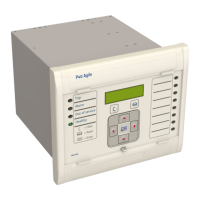
2.1 Overview of Hardware Design
The P253 hardware design overview is explained with the help of the schematic diagram. The P253
hardware consists of three sets of internal Current Transformers (CTs). These internal CTs are
designed to cater to protection & metering requirements. Dedicated CT is available for the earth fault
protection requirements. The relay also has provision for the built-in SMPS unit which accepts power
supply input of 24-230 V AC/DC from external source and outputs 12 V and 24 V DC for internal
circuitry. The current signals acquired as analogue inputs get processed through operational amplifier,
filter circuit, multiplexer, ADC (Analog to digital converter) and finally fed to CPU.
The CPU design is a hybrid of the digital signal processor (DSP) and high speed microcontroller which
runs complex algorithm for deriving the fundamental & harmonic component from the input current
signals. The digital inputs and outputs modules are designed to interface the monitoring, control and
protection signals through optically isolated circuit as per the field requirements. The other peripherals
modules like 16x2 LCD display, feather touch keys, USB and RS485 communication interfaces,
battery backup for RTC and built in memory circuits are integrated as per the schematic diagram and
enclosed in the IP-52 enclosure.
 Loading...