USB 3.0 Hub Design Guide
© 2015 Genesys Logic, Inc. - All rights reserved. Page 18
GLI Confidential
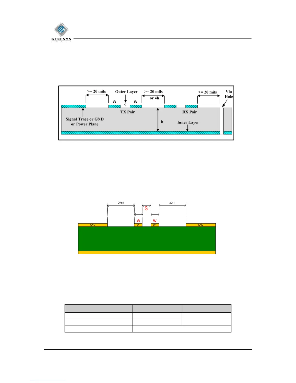
2.8 Trace Width and Adjacent Space Gap
2.8.1 USB 3.0
The edge-to-edge spacing of adjacent pairs should be greater than 20 mils at least. The differential pair traces
should be kept at least 20 mils away from the edge of the Power or GND plane (trace), signal trace and vias.
Figure 2.16
*Note: Different Port differential signal trace Gap ≥20 mils or use GND plane isolate, The GND plane and
differential signal trace Gap ≥20 mils.
2.8.2 USB 2.0
The GND of the signal lines shall have spacing of at least 20mil with the signal lines.
Figure 2.17
2.8.3 Recommend Width and Space for USB 2.0 & USB3.0 Trace
Please refer to the following table for the recommending width and spacing on 4-layer PCB setting:
*Note: The trace width (W) / spacing (S) may be different by PCB material characteristic base on PCB Vendor
suggest.