User Guide
GD32450Z-EVAL
24
5.8. ADC0_ADC1_Follow_up_mode
5.8.1. DEMO purpose
This demo includes the following functions of GD32 MCU:
Learn to use the ADC to convert analog signal to digital data
Learn to use ADC0 and ADC1 follow-up mode
5.8.2. DEMO running result
Jump the JP13 to USART with the jumper cap, and then download the program
<08_ADC0_ADC1_Follow_up_mode> to the board. Connect serial cable to COM0, open
the HyperTerminal. PC5 pin connect to the external voltage input. PC3 is the output
voltage of the slide rheostat VR1 on board. Keep PC5 pin should not be reused by other
peripherals. JP17 should not be connected.
TIMER1_CH1 is the trigger source of ADC0 and ADC1. When the rising edge of
TIMER1_CH1 coming, ADC0 starts immediately and ADC1 starts after a delay of several
ADC clock cycles. The values of ADC0 and ADC1 are transmitted to array adc_value[0]
and adc_value [1] by DMA.
When the first rising edge of TIMER1_CH1 coming, the value of the ADC0 conversion of
PC3 pin is stored into the low half word of adc_value [0], and after a delay of several ADC
clock cycles the value of the ADC1 conversion of PC5 pin is stored into the high half word
of adc_value [0]. When the second rising edge of TIMER1_CH1 coming, the value of the
ADC0 conversion of PC5 pin is stored into the low half word of adc_value [1], and after
a delay of several ADC clock cycles the value of the ADC1 conversion of PC3 pin is
stored into the high half word of adc_value [1].
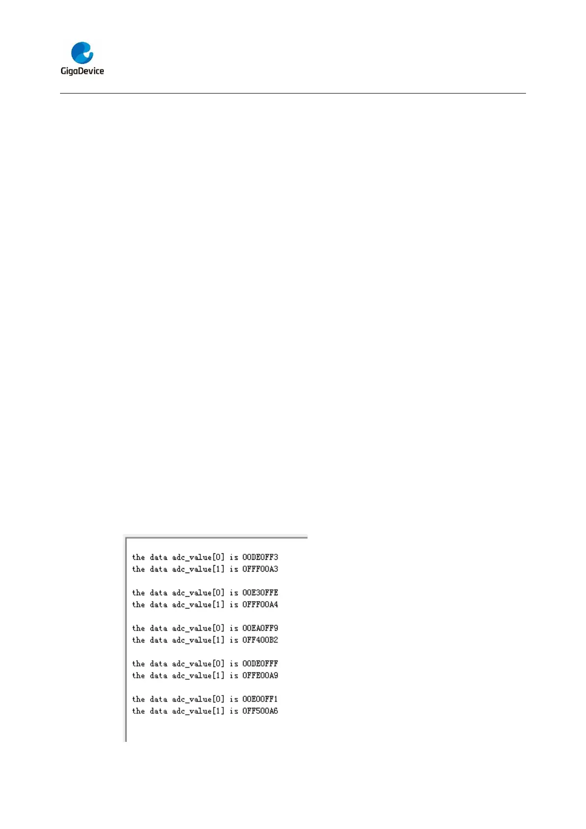
When the program is running, HyperTerminal display the regular value of ADC0 and
ADC1 by adc_value [0] and adc_value [1].


 To Next Page