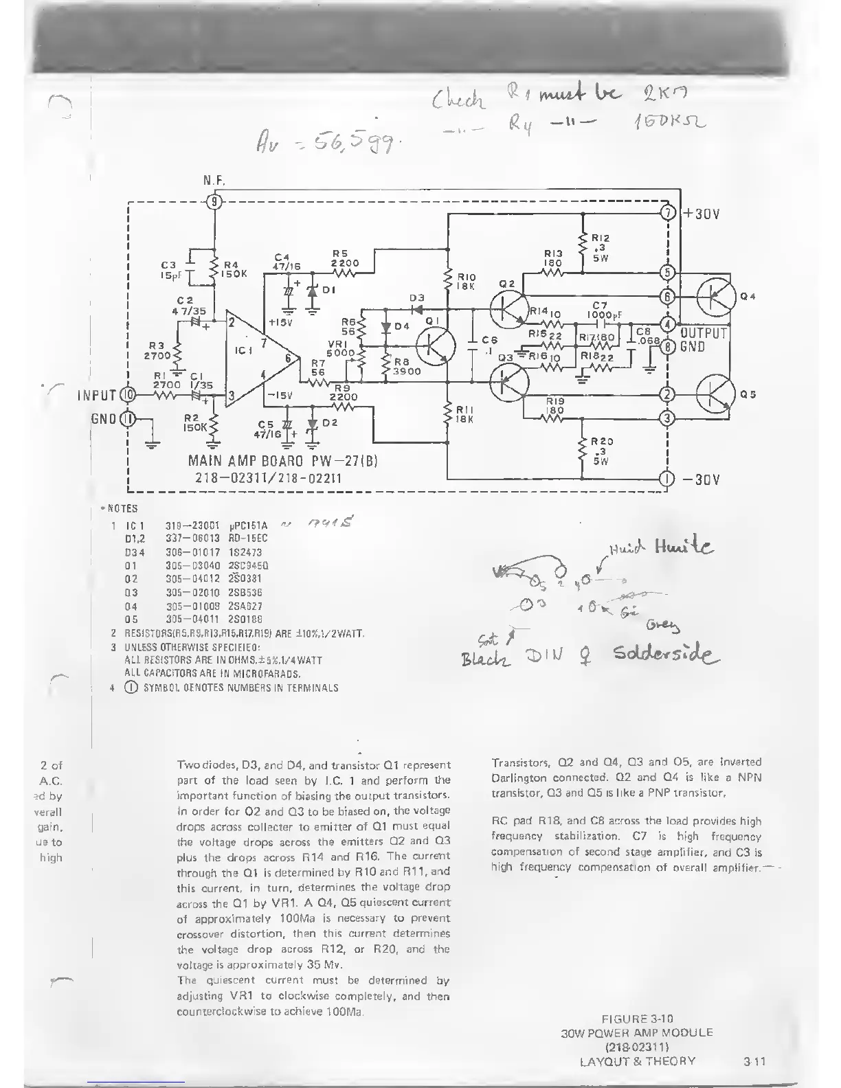
TES
IC 1
319-
230D1
pPC151A
D1.2
337-
06013
R0-15EC
03.4
3Q6-
01017 1S2473
01
305-
03040
2SC945Q
02
305- 04012 2"SG331
03
305-
02010 2SB53E
04
305-
01003 2SAG27
Q5
305-
04011 2SD188
2
RES!ST0.ftSlR5.R3.R13.Rl5,R!7.R19l ARE ±10%,1/2WATT.
3 UNLESS
OTHERWISE
SPECIFIED:
ALL RESISTORS ARE IN OHMS.
±5%. 1/4
WATT.
ALL
CAPACITORS ARE
IN MICROFARADS.
4
®
SYMBOL DENOTES NOMBERS
IN TERMINALS
S—
0w
*^
i 2
of
A.C.
?d by
veraM
gain,
ue
to
high
Two diodes. D3, and
D4. and transistor
Q1 represent
part of
the load
seen by l-C. 1 and
perform the
important
function of biasing the output
transistors.
In order for Q2 and Q3
to
be biased on,
the voltage
drops across collecter to
emitter of Q1
must
equal
the voltage drops
across the
emitters Q2
and Q3
plus the drops across R14
and R16.
The current
through the Ql is
determined by
R 10
and R1
1 ,
and
this
current, in turn,
determines
the voltage drop
across
the Ql by VR1.
A 04, Q5
quiescent current
of
approximately IQOMa
is necessary to prevent
crossover
distortion, then this current determines
the
voltage drop across R12, or R2D, and the
voltage
is approximately 35 Mv.
The
quiescent
current must
be
determined
by
adjusting VR1 to clockwise
completely, and then
counterclockwise to achieve lOOMa.
Transistors,
02 and Q4, 03 and Q5,
are Inverted
Darlington
connected. Q2 and Q4 is like a NPN
transistor, Q3
and
Q5
is like
a
PNP transistor.
RC pad R18,
and
C8 across the load provides
high
frequency stabilization.
C7 is high frequency
compensation of
second stage amplifier, and
C3 is
high frequency
compensation of overall
amplifier.—
FIGURE
3-10
30W
POWER
AMP
MODULE
(218-02311)
LAYOUTS
THEORY
3-11