A
J 301
-
©
G
®
Q)
E
CD
D
@
52473
2Z-12A
SC945G.
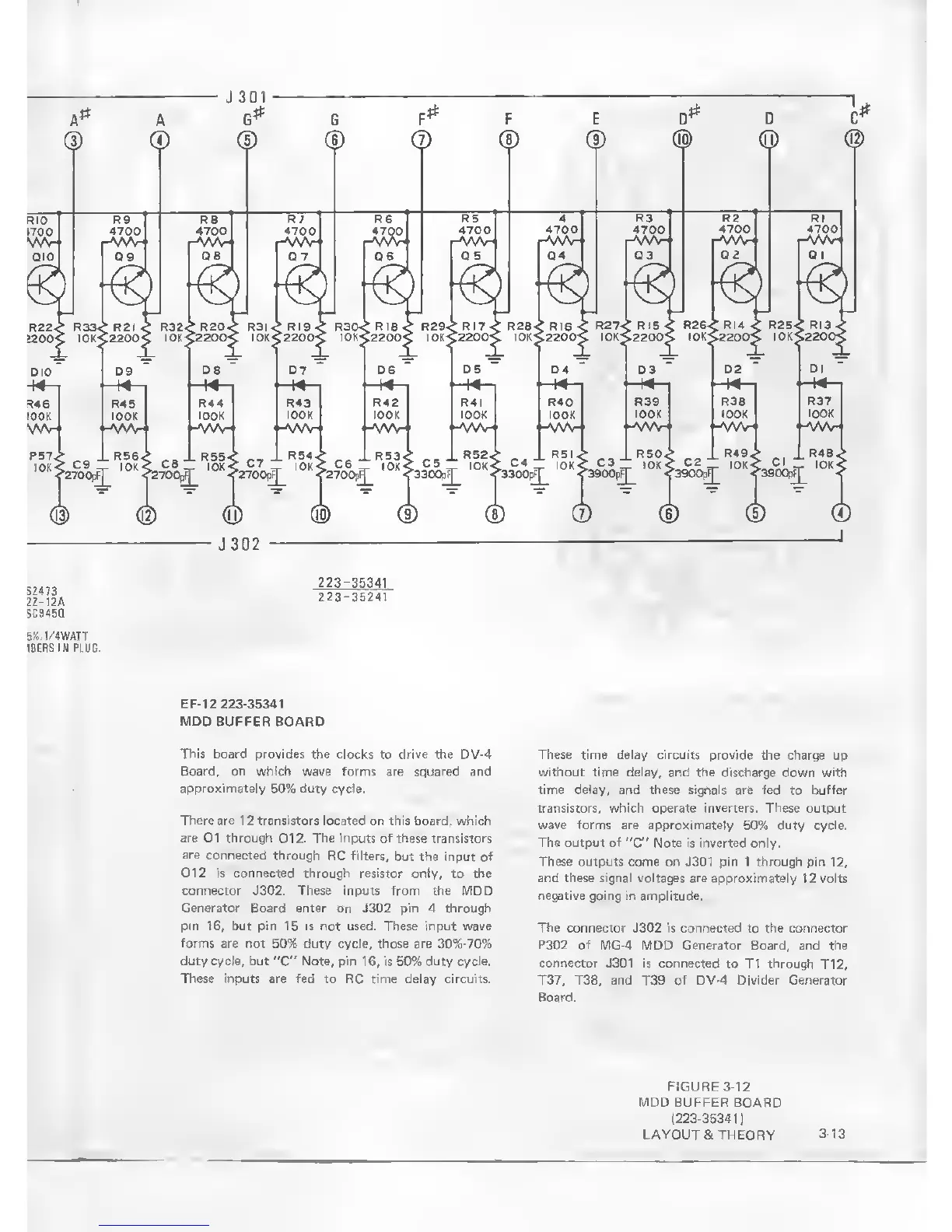
EF-12
223-35341
MDD BUFFER
BOARD
This
board provides the clocks to drive the
DV-4
Board, on which
wave
forms
are squared and
approximately 50% duty cycle.
There are
1 2
transistors
located on this board, which
are Q1 through
G12.
The inputs of these transistors
are
connected through
RC
filters,
but the input of
Q12 is connected through resistor only,
to
the
connector J302. These inputs from the MDD
Generator Board enter on J302 pin 4 through
pin 16, but pin 15 is not used. These input wave
forms are not 50% duty cycle, those are 30%-7G%
duty cycle, but
"C"
Note, pin
16,
is
50%
duty cycle.
These inputs are fed to RC time delay circuits.
These time delay circuits provide the
charge up
without
time delay, and the discharge down with
time delay, and these signals are fed
to
buffer
transistors,
which
operate
inverters. These
output
wave forms are approximately
50%
duty cycle.
The output of
"C"
Note
is
inverted
only.
These
outputs come on J301 pin 1 through pin
12,
and these signal voltages are approximately
12 volts
negative going in amplitude.
The
connector J302 is connected to the connector
P302 of
MG-4 MDD
Generator
Board, and the
connector
J301 is connected to
Tl
through
T12,
T37, T38, and T39
of
DV-4 Divider Generator
Board.
FIGURE
3 12
MDD BUFFER BOARD
(223-35341)
LAYOUT
& THEORY
3-13