•
NOTES
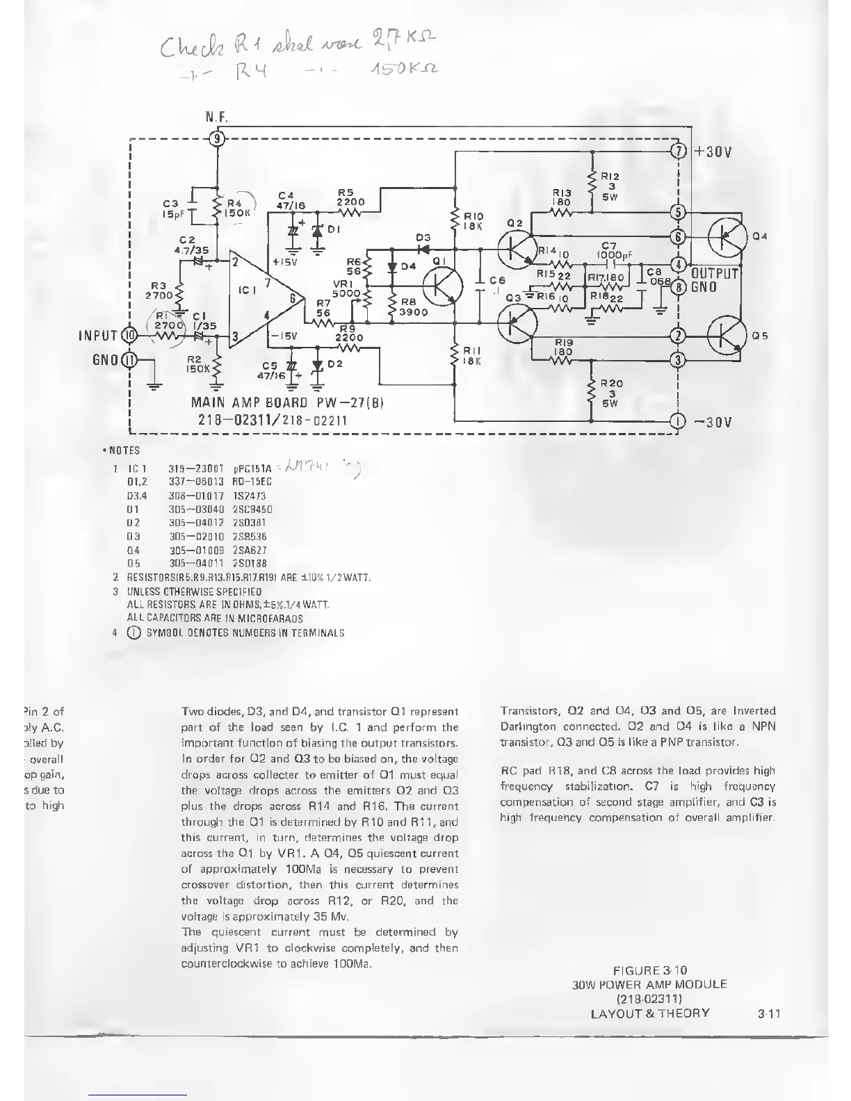
1 IC 1 319-23001 MPG151A
:
01.2
337-06013
R0-15EC
D3.4 306-01017
1S2473
D1
305-03040
2SC9450
Q2
305-04012
2S0381
Q3 305-D201D 2SB536
04 3D5—
O10O9
2SA627
05
3O5-040I1
2SD188
2 RESIST0RS(R5.R9.fil3.R15.R17.R19) ARE
±10%.
V2WATT.
3 UNLESS OTHERWISE
SPECIFIED:
ALL RESISTORS
ARE
IN DHMS;±5%.1/4WATT.
ALL CAPACITORS
ARE
IN MICROFARADS.
4 (T)
SYMBOL DENOTES
NUMBERS IN TERMINALS
3
in
2
of Two diodes, D3, and D4, and transistor Q1 represent
Transistors, Q2 and Q4, Q3 and Q5, are Inverted
ily
A.C.
part
of
the load seen by I.C. 1 and perform the
Darlington connected.
02 and 04 is
like
a NPN
ailed by important function of biasing the output transistors.
transistor, Q3 and
05
is like a PNP transistor,
overall
In order for 02 and Q3 to be biased on, the voltage
op
gain,
drops across collector
to
emitter of
01 must
equal
RC
P
ad R1S
-
and CS across the load
P
rovides h
'B
h
s
due
to the voltage drops across the emitters
Q2
and Q3
frequency
stabilization. C7 is
high
frequency
to high
plus the drops across R14 and
R16.
The current
compensation of
second stafle
amplifier, and
C3 is
through the 01 is determined
by R10
and
R1
1,
and
hi
9
h frequency compensation of overall amplifier.
this current, in turn, determines the voltage drop
across the Q1 by VR1.
A Q4,
Q5 quiescent current
of
approximately
lOOMa is necessary to prevent
crossover distortion, then this current determines
the voltage drop across R12, or R20, and the
voltage is approximately
35
Mv,
The quiescent current
must
be determined by
adjusting VR1 to clockwise completely, and then
counterclockwise to achieve
1D0Ma.
FIGURE 3 10
30W
POWER AMP
MODULE
(218-02311)
LAYOUT
&
THEORY 3-11
 Loading...