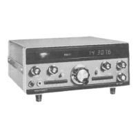
Page 293
11
3
10 4
11
3
10
4
11
3
10
4
11
3
10 4
11
3
10 4
LOWER SIDEBAND PRESET.
NUMERICALVALUE 8421
8421
8421
8421
8421
LOGICALVALUEXLHHL LHHL
LLLL
LHHL LHLL
Figure
46
PRESET VALUE
6
6
0
6
4
*
L=LOW H~HIGH,
LOWS NOTSIGNIFICANT
TOTAL OF HIGH VALUES
EQUAL PRESET VALUE.
display
is
13900.0 kHz as shown in Figure 4.5. However, as
there is no provision for displaying the figure
"1," the
display will read 3900.0. which is the correct signal
frequency. The following tabulation shows the calculations:
HFO for 3.5 MHz band
12395.0 kHz
VFO 51 01.4
Premix 7293.6 kHz
False zero 10000.0 kHz
IC106:
All pins are grounded and are therefore low,
so
the preset value is 0.
IC104: Pin 11
is
grounded directly and pin 4 is
grounded through
R107, so there is no value
at
these pins. When the front panel LSB button is
pushed, a positive voltage is connected to pin 22
of counter circuit board A. This voltage is
applied to the anodes of
0105 and 13102, which
carses them to conduct and pass the voltage to
pins 3 and 10 of the IC. These pins are therefore
high and have values of 4 and 2,
so
the preset
value of the
IC
is
6.
BFO for LSB
Preset
3393.6
-
6606.4 kHz
IC102:
Pin 11
is
grounded directly, and pins 10 and
4
are grounded through R105 and R104. so these
Reset frequency 6606.4 kHz
Counted frequency (Premix)
7293.6
Display (Signal) frequency '13900.0 kHz
'The signal frequency will be displayed
as"3900." as
the "1" cannot
be
seen.
NOTE: The first of the six display digits is controlled by the
BAND switch and is blank, 1, or 2 as appropriate. This
discussion deals only with digits two through six, controlled
by the counter
la.
BCD (binary-coded decimal)
is
used to program each
counter
IC for
a
preset frequency
at
pins 11. 3. 10, and 4
(which have decimal values of 8, 4,
2,
and 1). If any of these
pins is grounded,
it
is
logically low, and if not connected or
positive,
it
is logically high. Only the high pins are
significant. The values of the highs, if any,
at
the pins of
each
IC are added together to determine the preset number
for that IC. Refer to Figure
4-6, the xhematic diagram, and
the following explanation of how the counter
IC's are
programmed for the
LSB preset frequency of 6606.4 kHz.
IC110:
Pins 11 and 4 are grounded and therefore have
no value. Pins 3 and 10, with values of 4 and 2
respectively, are not connected and are therefore
high.
so
the figures are significant. 4
+
2
=
6 as
the preset value for this
IC.
IClOB:
Same as ICllO.
pins are low and without value. The positive
LSB voltage is applied through
Dl09 to pin 3,
which becomes high and has a value of 4. The
preset value for this
IC is therefore 4.
The presets for the second, third and
fourth digits of the
display are fixed
as
"660"
(IC's 110, 108 and 106). The
remaining two digits change as the
US$, LSB, and
CW
buttons apply positive voltages through the diode matrix to
the pins of
IC104 and IC102. The USB preset frequency will
be 6603.6 because the positivevoltage from pin 23 of board
A
will be applied to IC104 pins 10 and 4, total value 3. and
IC102 pins 3 and 10, total value 6. The
CW
preset frequency
will be 6604.3 because the positive voltage will
be
connected
from pin 24 of board A to
IC104 pin 3, value 4. and to
IC102 pins 10 and 4, total value 3.
IC's 103, 105, 107. 109 and 111 are memory latches which
store data from the counters during counting periods. This
eliminates flashing digits which would otherwise be present
during counting periods. During the transfer pulse, the BCD
count present at a
counter output is transferred to the
memory, which retains
thecount at itsoutput until the next
transfer pulse.
The memory outputs
are
connected to the segment drivers,
which are located on the display circuit board. The
significant outputs are logically high. Each memory output
is
coded using BCD in a manner similar to the decimal
coding described for presetting the counters.