Rev. 1.20 10 January 23, 2015 Rev. 1.20 11 January 23, 2015
BS82B12A-3/BS82C16A-3/BS82D20A-3
Touch Key 8-Bit Flash MCU with LED/LCD Driver
BS82B12A-3/BS82C16A-3/BS82D20A-3
Touch Key 8-Bit Flash MCU with LED/LCD Driver
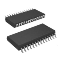
PA3/SDA/RX
PA0/TCK1/SCOM2/ICPDA/OCDSDA
BS82D20A-3/BS82DV20A-3
28 SOP-A/SSOP-A
PA2/SCOM3/ICPCK/OCDSCK
PA7/SCL/TX
VDD
VSS
PA1/SCOM0/KEY20
PA4/INT/TCK0/SCOM1/KEY19
PC7/TP0_1/SSEG15/KEY18
PC6/TP1_1/SSEG14/KEY17
PC5/SSEG13/KEY16
PC4/SSEG12/KEY15
PC3/SSEG11/KEY14
PC2/SSEG10/KEY13
PC1/SSEG9/KEY12
PC0/SSEG8/KEY11
PB7/SSEG7/KEY8
PB6/SSEG6/KEY7
PB5/SSEG5/KEY6
PB4/SSEG4/KEY5
PB3/SSEG3/KEY4
PB2/SSEG2/KEY3
PB1/SSEG1/KEY2
PB0/SSEG0/KEY1
PD1/TP0_0/SSEG17/XT2
PD0/TP1_0/SSEG16/XT1
PD2/SSEG18/KEY10
PD3/SSEG19/KEY9
28
27
26
25
24
23
22
21
20
19
18
17
16
15
1
2
3
4
5
6
7
8
9
10
11
12
13
14
Note:1.Ifthepin-sharedpinfunctionshavemultipleoutputssimultaneously,itspinnamesattherightsideofthe
"/"signcanbeusedforhigherpriority.
2.TheOCDSDAandOCDSCKpinsaretheOCDSdedicatedpinsandonlyavailableforthe
BS82BV12A-3,BS82CV16A-3andBS82DV20A-3devices,whicharetheOCDSEVchipsforthe
BS82B12A-3,BS82C16A-3andBS82D20A-3devicesrespectively.
Pin Descriptions
Withtheexceptionofthepowerpinsandsomerelevanttransformercontrolpins,allpinsonthe
devicecanbereferencedbytheirPortname,e.g.PA0,PA1,etc,whichrefertothedigitalI/O
functionofthepins.HoweverthesePortpinsarealsosharedwithotherfunctionsuchastheTouch
Keyfunction,TimerModules,etc.Thefunctionofeachpinislistedinthefollowingtables,however
thedetailsbehindhoweachpiniscongurediscontainedinothersectionsofthedatasheet.
AsthePinDescriptiontableshowsthesituationforthepackagewiththemostpins,notallpinsin
thetablewillbeavailableonsmallerpackagesizes.
BS82B12A-3
Pin Name Function OP I/T O/T Description
PA0/TCK1/
SCOM2/
ICPDA/
OCDSDA
PA0
PAWU
PAPU
ST CMOS
General purpose I/O. Register enabled pull-up and wake-up.
TCK1 PTM0C0 ST — PTM0 clock input
SCOM2 SLCDC0 — SCOM LCD driver output for LCD panel common
ICPDA — ST CMOS In-circuit programming address/data pin
OCDSDA — ST CMOS On-chip debug support data/address pin, for EV chip only.
PA1/SCOM0
PA1
PAWU
PAPU
ST CMOS
General purpose I/O. Register enabled pull-up and wake-up.
SCOM0 SLCDC0 — SCOM LCD driver output for LCD panel common
PA2/
SCOM3/
ICPCK/
OCDSCK
PA2
PAWU
PAPU
ST CMOS
General purpose I/O. Register enabled pull-up and wake-up.
SCOM3 SLCDC0 — SCOM LCD driver output for LCD panel common
ICPCK — ST — In-circuit programming clock pin
OCDSCK — ST — On-chip debug support clock pin, for EV chip only.
 Loading...