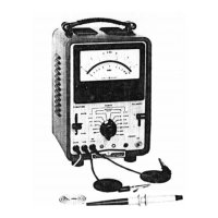
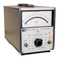
Model
412A
Section
VI1
C
7-1.
I
NTR
0
D
U
CTI
0
N
,
SECTION
VI1
RCUIT
DIAGRAMS
Figures 7-1 and 7-2 give the location
of
other components
within the cabinet model and rack
model
instruments,
7-2. This section contains information necessary
to
respectively.
Figure
74
is a schematic diagram
of
the
Model
maintain the
Model
412AIAR. Figure
7-3
shows the 412A/AR, and includes pictorial views
of
the circuit
location
of
components mounted on the range switch. boards.
NOTES
1.
COMPONENT VALUES SHOWN
AS
FOLLOWS UNLESS OTHERWISE NOTED.
RESISTANCE
IN
OHMS
CAPACITANCE IN MICROFARADS
2.
h
DENOTES CIRCUIT COMMON.
3.
&
DENOTES POWER LINE GROUND.
4.
--
DENOTES ASSEMBLY.
5.
DENOTES MAIN SIGNAL PATH.
6.
-
DENOTES FEEDBACK PATH.
7.11
DENOTES FRONT PANEL MARKING.
8.
c
L,
1
DENOTES REAR PANEL MARKING.
9.
DENOTES SCREWDRIVER ADJUST.
10.
y
AVERAGE VALUE
SHOWN,
OPTIMUM VALUE SELECTED AT FACTORY.
11.
DC VOLTAGES MEASURED WITH RESPECT TO CIRCUIT COMMON
(A),
LINE VOLTAGE AT
115
V, AND
NO
METER DEFLECTION.
7-1
00
1
29-5