Technical Reference Guide www.hp.com 5-3
Input/Output Interfaces
IDE Bus Master Control Registers
The IDE interface can perform PCI bus master operations using the registers listed in Table 5-2.
These registers occupy 16 bytes of variable I/O space set by software and indicated by PCI
configuration register 20h in the previous table.
NOTE:
Unspecified gaps are reserved, will return indeterminate data, and should not be written to.
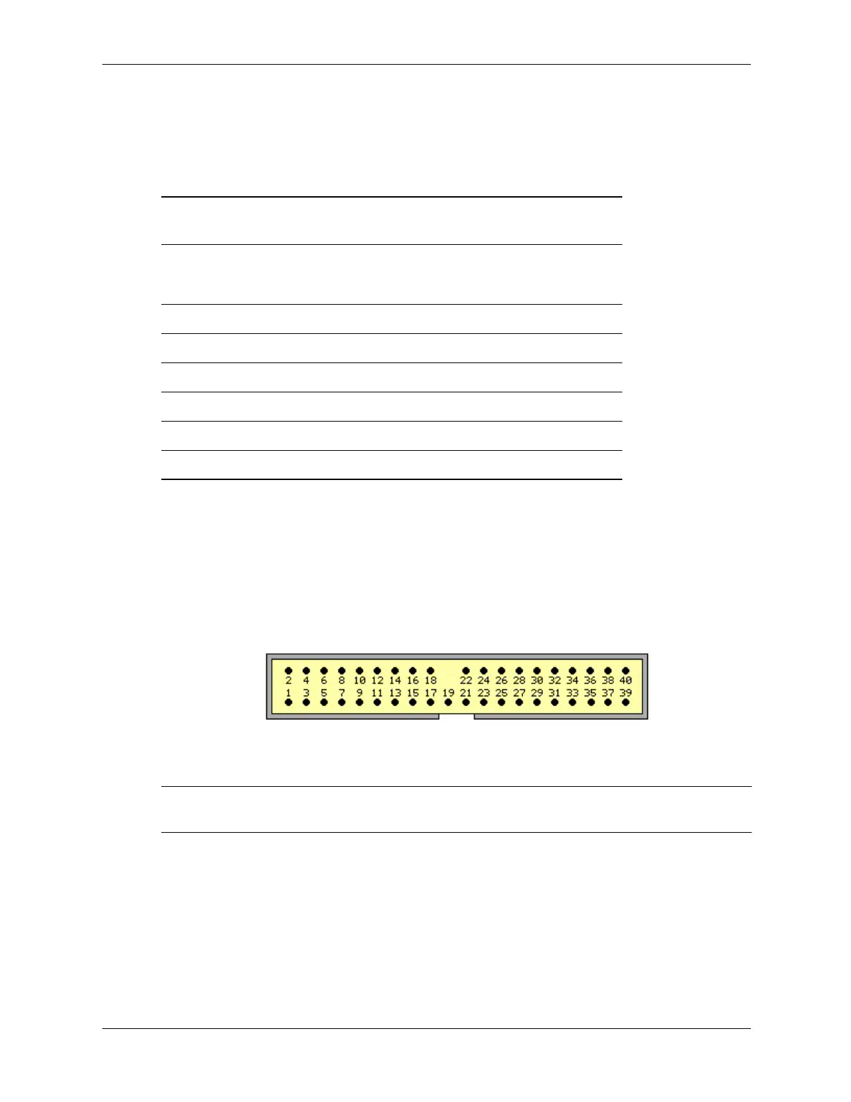
IDE (PATA) Connector
The SFF, ST, MT, and CMT form factors provide a standard 40-pin connector for a primary IDE
device and in most factory configurations connects to a optical drive (CD or DVD). Some signals
are re-defined for UATA/33 and higher modes. Device power is supplied through a separate
connector.
Figure 5-1. 40-Pin IDE (PATA) Connector.
✎
The USDT form factor does not include 40-pin IDE connctor. The IDE interface and hard drive
power signals are both a part of the MultiBay interface used on the USDT form factor.
Table 5-2.
IDE Bus Master Control Registers
I/O
Address
Offset
Size
(Bytes) Register
Default
Value
00h 1 Bus Master IDE Command (Primary) 00h
02h 1 Bus Master IDE Status (Primary) 00h
04h 4 Bus Master IDE Descriptor Pointer (Pri.) 0000 0000h
08h 1 Bus Master IDE Command (Secondary) 00h
0Ah 2 Bus Master IDE Status (Secondary) 00h
0Ch 4 Bus Master IDE Descriptor Pointer (Sec.) 0000 0000h
 Loading...