Q1
2
3
1G
D
S
33pFC14
C13 33pF
C11 33pF
R16 0
0R17
R15 0
D1
R23 0
1V8(3V3)
100KR4
R3 100K
R13 0
1uFC8
Q3
2
3
1G
D
S
C1
1uF
C3
22uF
J1
7776
74
72
70
68
66
64
62
60
58
56
54
52
50
48
46
44
42
40
38
36
34
32
30
28
26
24
22
20
10
8
6
4
2
75
73
71
69
67
65
63
61
59
57
55
53
51
49
47
45
43
41
39
37
35
33
31
29
27
25
23
21
11
9
7
5
3
1
P1
P3
P5
P7
P9
P11
P21
P23
P25
P27
P29
P31
P33
P35
P37
P39
P41
P43
P45
P47
P49
P51
P53
P55
P57
P59
P61
P63
P65
P67
P69
P71
P73
P75
P2
P4
P6
P8
P10
P20
P22
P24
P26
P28
P30
P32
P34
P36
P38
P40
P42
P44
P46
P48
P50
P52
P54
P56
P58
P60
P62
P64
P66
P68
P70
P72
P74
M1 M2
C4
220uF
C2
100nF
D2
61
3 4
2 5
C15 33pF
C17 33pF
470pFC18
C19 33pF
0R12
33pFC16
100KR2
10KR24
R5 100K
33pFC9
1V8
R6 10K
200R8
VBAT
R11 0
0R14
33pFC12
J2
11
7
3
6
2
5
1
4
10
9
8
S2
S3
M1
CD
VCC
GND
RST
VPP
CLK
I/O
M2
Q2
2
3
1G
D
S
VBAT
VBAT
R9 1M
R19
0
C7
330pF
C10 2.2pF
R20 0
1M
R22
V-gpio1
Q4
2
3
1G
D
S
R21 0
Vgpio2
ANT_TUNE_2
ANT_TUNE_2
ANT_TUNE_3
ANT_TUNE_3
ANT_TUNE_1
ANT_TUNE_1
ANT_TUNE_0
ANT_TUNE_0
GPS_DISABLE
USIM_RESET
USIM_RESET
USIM_CLK
USIM_CLK
USIM_IO
USIM_IO
USIM_DET
USIM_DET
CONFIG3
CONFIG3
CONFIG2
CONFIG2
CONFIG1
CONFIG1
CONFIG0
CONFIG0
USB_DP
USB_DP
WAKE_On_WWAN
W_DISABLE
LEDUSB_DM
USB_DM
USIM_PWR
USIM_PWR
GPIO1
GPIO2
GPIO2
VBAT
POWER_ON_OFF
POWER_ON_OFF
RESET
RESET
BODYSAR_N
Capacitor of D2 should be less than 10pF
V-gpio2 is power supply of GPIO2 domain
DNI
DNI
DNI
1.8V (3.3V), active low
1.8V, Active Low
Cap close to pin67
When VBAT is always on, must use this design
1.8V tolerence
ME906s is configed as WWAN-SSIC0 internally
CONFIG[3:0] to PC
USB eye debug.
to PC USB2.0 interface
When module on/off is controlled only by VBAT, must use this design
Power_on_off control option 1
RF on: light on
R24 should not be larger than 10K
RF off: light off
1.8V(3.3V),active low
V-gpio1 is power supply of GPIO1 domain
DNI
DNI
DNI,Reserve for
RC is reserved for RF debug
When use option 1 , R23 must be DNI
USIM absent: CD-->GND;
other devices: for GCF or PTCRB debug.
USIM present: CD Open
C18:to avoid twitter
Tunable antenna SCH
When use option 2 , R24 must be DNI
USB SCH
Config pin SCH
GPIO2 is from SOC
Power_on_off control option 2
GPIO1 is from SOC
#
0402
When Vgpio2 is ON
Q1 is on and Q2 is off
1.8V (3.3V),open drain ,active low
from proximity sensor
Power_On_Off is controlled by GPIO2
1.8V(3.3V),active low
CONFIG[3:0] is for card type indication and present detection
1.8V(3.3V).high:on,low:off
Power_On_Off is is pulled LOW
DNI: Do Not Install initially.
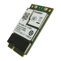
M.2: new name of NGFF.
Note: If M1 and M2 pin is metal,you can connect it to GND
GND of socket should be wellconnected to module GND
#
Q1 is off and Q2 is on
When Vgpio2 is off
Module is shut off safely
RESET control SCH
USIM SCH
#
1.8V or 3.0V
#
USIM_PWR:
#
Module output: 0V or NC
#
current: 2.5A max
M.2: 3.135V-4.4V,typical 3.3V
One 220uF Tantalum Capacitor is needed to
below 3.135 V in any case.
make sure that the voltage does not drop
USIM_DET Must Be Used.

 Loading...