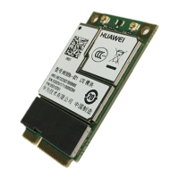
HUAWEI ME906s LTE M.2 Module
Hardware Guide
Huawei Proprietary and Confidential
Copyright © Huawei Technologies Co., Ltd.
Tunable Antenna control (4 GPIOs)
MAIN and AUX (supports Diversity and GPS simultaneously)
Supports MO and MT
Supports formats of PDU
Point-to-point and cell broadcast
GPRS: DL 85.6 kbit/s; UL 85.6 kbit/s
EDGE: DL 236.8 kbit/s; UL 236.8 kbit/s
WCDMA CS: DL 64 kbit/s; UL 64 kbit/s
WCDMA PS: DL 384 kbit/s; UL 384 kbit/s
HSPA+: DL 21.6 Mbit/s; UL 5.76 Mbit/s
DC-HSPA+: DL 42 Mbit/s; UL 5.76 Mbit/s
LTE FDD: DL 150 Mbit/s; UL 50 Mbit/s @20M BW cat3
Windows 7/8/8.1/10, Android 4.0 or later
[1]: When the ME906s module works at –20°C to –10°C or +55°C to +70°C , NOT all its RF
specifications comply with the 3GPP specifications.
2.3 Circuit Block Diagram
The ME906s module is developed based on Huawei's Balong Hi6921M platform.
Figure 2-1 shows the circuit block diagram of the ME906s module. The application
block diagram and major functional units of the ME906s module contain the following
parts:
Baseband controller

 Loading...