HUAWEI ME909u-521 LTE LGA Module
Hardware Guide
Description of the Application Interfaces
Huawei Proprietary and Confidential
Copyright © Huawei Technologies Co., Ltd.
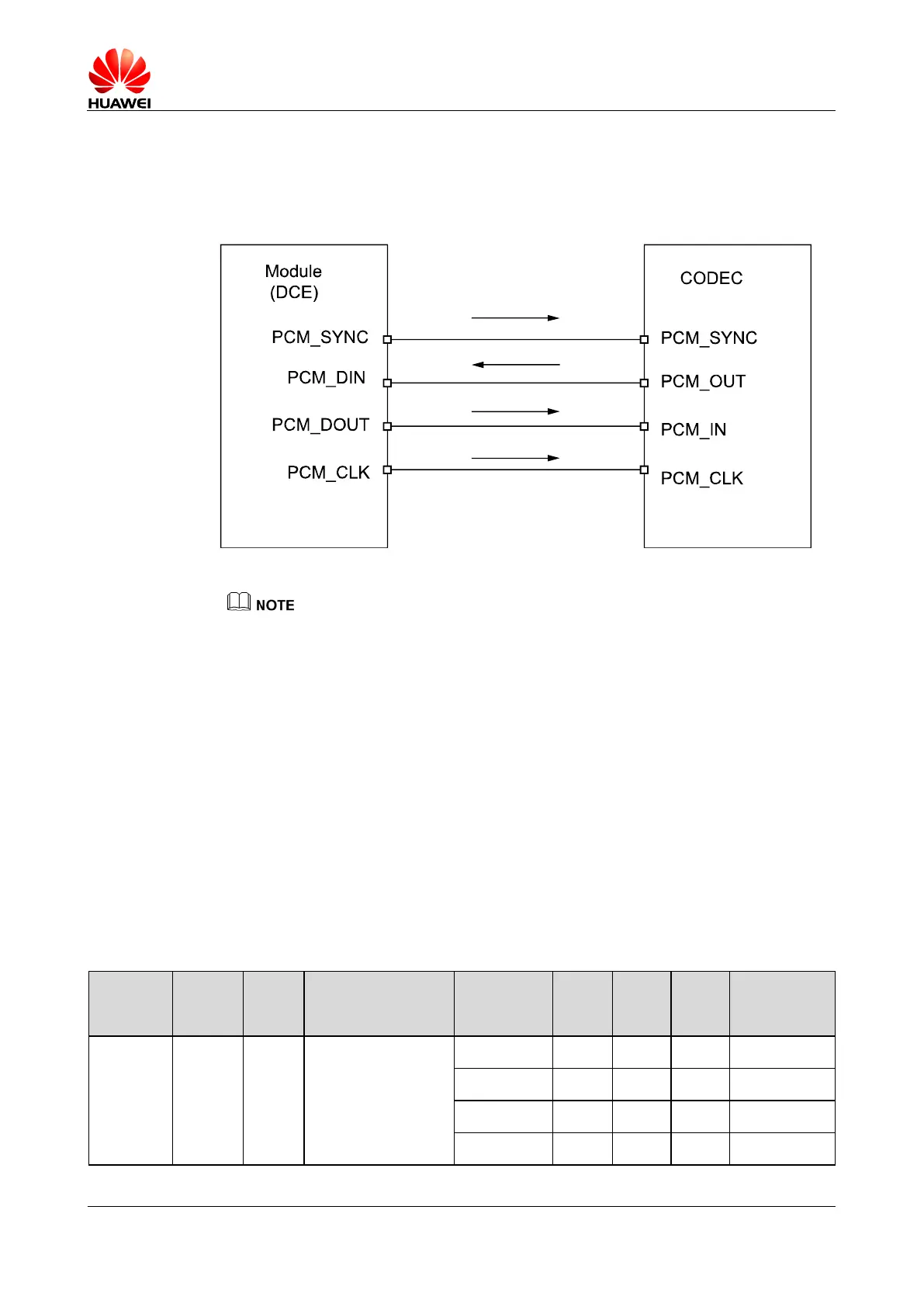
The ME909u-521 module PCM interface enables communication with an external
codec to support linear format.
Figure 3-17 Circuit diagram of PCM interface (ME909u-521 module is used as PCM
master)
PCM_SYNC: Output when PCM is in master mode;
PCM_CLK: Output when PCM is in master mode;
The PCM function of ME909u-521 module is only supported in master mode.
It is recommended that a TVS be used on the related interface, to prevent electrostatic
discharge and protect integrated circuit (IC) components.
The signal level of CODEC must match that of the ME909u-521 module.
3.9 General Purpose I/O Interface
The ME909u-521 module provides GPIO pins for customers to use for controlling
signals which are worked at 1.8 V CMOS logic levels. Customers can use AT
command to control the state of logic levels of GPIO output signal. About the details of
GPIO command, see the HUAWEI ME909u-521 LTE LGA Module AT Command
Interface Specification.
Table 3-10 Signals on the GPIO interface
General Purpose I/O
pins. The function of
these pins has not
been defined.




 To Next Page