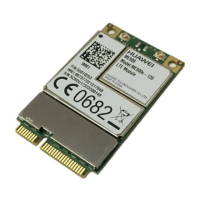
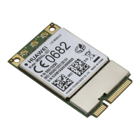
HUAWEI ME909u-521 LTE LGA Module
Hardware Guide
Mechanical Specifications
Huawei Proprietary and Confidential
Copyright © Huawei Technologies Co., Ltd.
Figure 6-3 Footprint design of customer’s PCB (Unit: mm)
The RF pad difference is the most important difference between HUAWEI LGA
modules, please refer to HUAWEI 30 mm x 30 mm LGA Module Hardware Migration
Guide.
6.7.3 Solder Mask
NSMD is recommended. In addition, the solder mask of the NSMD (Non-solder Mask
Defined) pad design is larger than the pad so the reliability of the solder joint can be
improved.
The solder mask must be 100 µm–150 µm larger than the pad, that is, the single side
of the solder mask must be 50 µm–75 µm larger than the pad. The specific size
depends on the processing capability of the PCB manufacturer.
6.7.4 Requirements on PCB Layout
To reduce deformation, a thickness of at least 1.0 mm is recommended.
Other devices must be located more than 3 mm (5 mm recommended) away from
the two parallel sides of the LGA module (rework requirement), and other sides
with 0.6 mm. The minimum distance between the LGA module and the PCB edge
is 0.3 mm.
When the PCB layout is double sided, the module must be placed on the second
side for assembly; so as to avoid module dropped from PCB or component
(located in module) re-melding defects caused by uneven weight.
 Loading...

