TC-508 Service Manual
11
Circuit Description
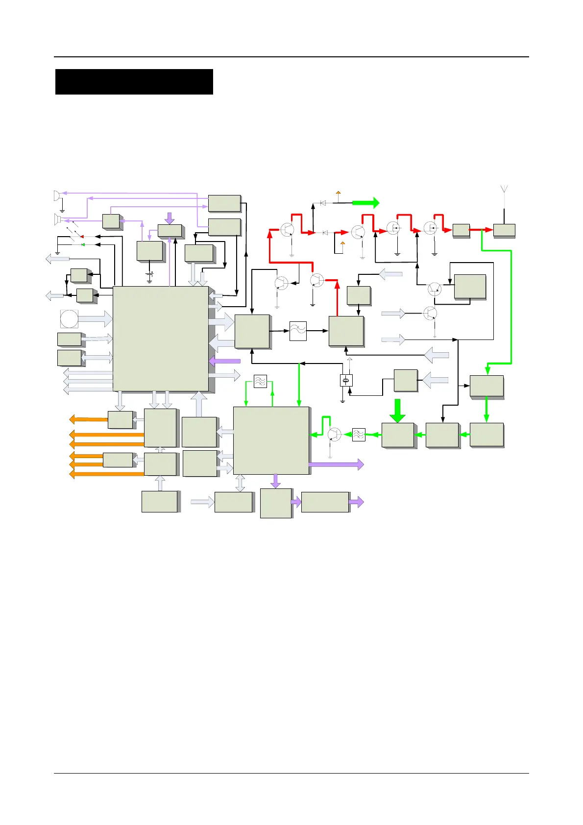
1. General Diagram
The general circuit is composed of TX section, RX section, Power Supply circuit, Control circuit and so
on. See the block diagram as shown below:
U601
MCU
SRT3210
PLL
U102
MB15E03S
L
TX/RX
VCO
Q102
POWER
MATCH
ANT LPF
BPF1
BPF2
MIXER
Q502
2SK318
LNA
Q501
AT41511
DEMODULATING IC
U611
BA4116FV
IF2 FILLER
CF501
450KHz
QT_MOD
E FILLER
R103
C132
DEMODULATING
CIRCUIT
CD501,R502,
C536
MICJACK
VOX_DET
Q611
D616
R204
C204
C205
R607
R632
R206
AF AMP
U302
SW
VOLUME
S201
SW_CHANNAL
RESET IC
U605
E2ROM
U603
LDO
U604
LDO
U602
LDO
U606
V_BAT
PLL
LOOP FILTER
APC
U401
1
3
2
4
SQUELCH DET
CIRCUIT
R562
C597
BUSY
DATA/STB/CK
LD
TX_CTL
SAVE
VT
VR SW
Q604
Q305
V_SAVE
V
R
SDA/SCL
R
E
S
E
T
EC0/EC1/EC2/EC3
M
O
D
E
AF
VOX
1
2
PTT/SK1/SK2
APC
VT
LO
QT_OUT
LO
TC-500S Block Diagram
MIC IN
CP
VR
VT
RX_TL
VCC
VDD
POWER AMP
Q403
RD07
POWER AMP
Q402
RD01
POWER AMP
Q401
2SC4226
LOCAL OSCILLATOR AMP
Q406
2SC4226
BUFFER AMP
Q105
2SC4226
LOCAL OSCILLATOR AMP
Q104
2SC5108
SW
Q405
DTC114EE
IF1 AMP
Q506
R_LED
T_LED
LED
D601
LED
D602
VDD
SPK
MODE_OUT
RXD
TXD
SP_JACK
J3
PJ-D3027D
1
2
MIC
B201
QT_OUT
M
O
D
E
T/R
T/R SW
Q103
D105
QT_OUT
NOISE FILLER
CIRCUIT
R509
C553
R510
FIL IN
FIL OUT
IF1 FILLER
XF501
38.85MHz
Crystal
XT 101
38.4MHz
VR SW
D405
VT SW
D404
QT_MODULATING
FILLER
AF_MODULATING
FILLER
APC_SW
Q404
DTC114YE
APC
T/R
BATTERY
G602
5V
N-DET
AF
AF AMP
U613
TA75S01F
AF PROCESSING
CIRCUIT
U610 ,C554,R538
AF
QT-AF
AF
QT-AF
W/N
W/N
AF_SW
Q302
BEEP
BEEP
AF_MUTE
RF_MUTE
Figure 1
TX Section: The audio signal from MIC is sent to the MCU chip (U601) directly. The baseband
signal processing circuit in U601 converts the amplified audio signal to digital signal via A/D conversion,
and then converts the digital signal to analog audio signal via D/A conversion after all processing
procedures such as filtering, signal compression, pre-emphasis, TX gain control and amplitude limiting
are completed. Then the audio signal from MCU passes through the low-pass filter circuit and goes to
VCO for direct frequency modulation. The modulated HF carrier signal passes through the buffer
amplifiers (Q104 and Q406), and goes to the amplifier (Q401) through the RF switch (D404). Then the
amplified RF signal enters the low-pass filter circuit after it is further amplified by the pre-driver (Q402)
and final-stage power amplifier (Q403), and then it will be finally transmitted via antenna after ultra
harmonics is removed.

 Loading...