3 - 11
Pin
No.
Line
Name
Description I/O
3 VBUS
VBUS connection detect for USB HUB.
H=USB connection detected.
I
8DAVOX
MIC signal detect.
H=Input detect.
I
9 CTFL CW TX status. I
11 RTKI
RTTY keying input.
H="Space" input.
I
12 UNLK
PLL (ADF4630) unlock detect.
L=Unlock detected.
I
13 DVOPT
Optional UT-121 installation detect.
H=Installed.
I
14 VSQM
Squelch level input. (MAIN BAND)
H=Squelch open.
I
15 VSQS
Squelch level input. (SUB BAND)
H=Squelch open.
I
16 RTDM
RTTY decode data from the DSP. (MAIN BAND)
I
17 RTDS
RTTY decode data from the DSP. (SUB BAND)
O
19,
20
MHSK0,
MHSK1
Handshake signal from the DSP. (MAIN
BAND)
I
21,
22
SHSK0,
SHSK1
Handshake signal from the DSP. (SUB
BAND)
I
23 FRES Front CPU reset signal. O
26 HIFOP1K
Optional IF filter (bandwidth=6 kHz)
installation detect.
L=Installed.
O
27 HIFOP2K
Optional IF filter (bandwidth=3 kHz)
installation detect.
L=Installed.
O
28
DVMTXCK
TX clock to CMX589 modem. O
29
DVMTXDT
TX data to the CMX589 modem. O
30
DVMRXCK
RX clock to the CMX589 modem. O
31
DVMRXDT
RX clock from the CMX589 modem. I
33 UDTXD Data output port for [USB] connector. O
35 PWRS
Transceiver power ON/OFF control.
H=Power ON.
O
36 UPWS
USB HUB power control.
H=USB power ON.
O
37 H8_CS6#
Dual-port SRAM chip select signal.
L=Selected.
O
38 H8_CS7#
Expander chip select signal.
L=Selected.
O
42 PCK PLL serial clock. O
43 PDAT PLL serial data. O
44 PSL PLL strobe. O
45 PST PLL strobe output. O
46 SKYS
Straight key/electronic keyer input. (A/D)
L=Key down.
I
47 EXRL
External SEND reray output.
H=Relay ON
O
48 ESTA
External tuner "START" signal output.
L=Tuning start.
O
49 EKEY
External tuner "KEY" signal input.
L=While tuning/tune NG.
I
51 MCK Common serial clock. O
52 MDAT Common serial data. O
53 TCON External tuner conection detect. I
54 CTXD CI-V (UART) output. O
55
CRXD/
CBSY
CI-V (UART) input/CI-V bus busy input.
L=Data "1" /Busy.
I
56
PCK/
CON0
DDS clock. O
Pin
No.
Line
Name
Description I/O
56 DSPCK DSP clock. O
57 DSPR DSP data. O
59 UDRXD USB data input. I
60 MSPK
[EXT-SP] (MAIN BAND) connection detect.
H=Connected.
I
61 SSPK
[EXT-SP] (SUB BAND) connection detect.
H=Connected.
I
63
AMBESTB
AMBE strobe to the optional UT-121. O
65
AMBERES
Reset signal to the optional UT-121. O
66
AMBECLK
AMBE clock to the optional UT-121. O
67
AMBETXD
AMBE serial data to the optional UT-121. O
68
AMBERXD
AMBE serial data from the optional UT-121.
I
73–
80
H8_D8–
H8_D15
DSP address bus. O
82 TND QPSK (L) decode data. I
83 NSQ Noise pulse input. (MAIN BAND) I
84 PSENI
Microphone PTT input.
H=While transmitting.
I
85 TRAS SEND signal. O
88 H8_LWR#
(Bus control) "L" write signal.
L=While writing.
O
89 H8_HWR#
(Bus control) "H" write signal.
L=While writing.
O
89 H8_RD#
(Bus control) Read signal.
L=While reading.
O
90 PTRAS
PTT circuit control.
H=While transmitting.
O
92 RES
CPU reset.
H=Reset.
O
94 SENI
PTT/ACC SEND signal.
H=While transmitting.
I
105 DSKY
DSP CW/RTTY keying signal.
L=Key down/space.
O
104 NSQS Noise pulse input. (SUB BAND) I
105 DSKY CW/RTTY keying. O
107 DVC DV CODEC power supply control. O
113 MFMTL Tone signals. (MAIN BAND) I
114 SFMTL Tone signals. (SUB BAND) I
115 VOXL VOX level input. I
116 DPTL "SEND" signal input from the data socket. I
121 DX1M TX/RX DSP data. (MAIN BAND) I
122 DX1S TX/RX DSP data. (SUB BAND) I
123 OVDK
Over deviation detect.
L= Over deviation detected.
I
124 THRI
Internal tuner through signal.
H=Tuner through.
I
125 BEEP Beep audio. O
126 STON Side tone. O
133 LTXD
Data output (UART) for the communication
with the front CPU.
O
134 LRXD
Data input (UART) for the communication
with the front CPU.
I
135 PWRK [POWER] input. (Pull-up) I
137 EDT EEPRROM data. I/O
138 ECK EEPRROM clock. O
140 IKEY
Internal tuner "KEY" input (UART).
L=Tuner ON.
I
142 ISTA Internal tuner "START" signal (UART). O
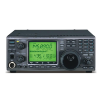
• MAIN CPU (MAIN UNIT: IC1201)

 Loading...