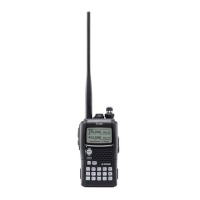
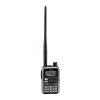
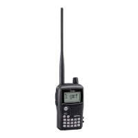
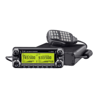
4 - 7
LINE
NAME
DESCRIPTION IN/OUT STATUS CONDITION
POWER [POWER] key input. (Pull-up). IN L –
PKEY [PWR] key input (Pull-up). IN L The key is pushed
DICK [DIAL] input(Phase A). IN – –
DIUD [DIAL] input(Phase B). IN – –
PTT [PTT] key input (Pull-down). IN H The key is pushed
SQL [SQL] key input (Pull-up). IN L The key is pushed
I0–I3 Initial matrix ports. IN – –
KR0–KR4
Key detect signal.
(Pushed bottom is detected according to the input voltage.)
IN – –
KS0–KS3 Key matrix ports. OUT – –
ESIO Serial data to the EEPROM. IN/OUT – –
ECK Clock to the EEPROM. OUT – –
TXC T6 line regulator (M: Q650–652) control signal. OUT H While transmitting.
BLED [BUSY] LED driver (L: Q201) control signal. OUT H RX(Squelch open)
LIGHT LCD/Key backlight driver (L: Q202) control signal. OUT L Lights ON.
LCDDT Serial data to the LCD driver (L: DS1). OUT – –
LCDCS Chip select signal to the LCD driver (L: DS1). OUT – –
LCDCK Clock to the LCD driver (L: DS1). OUT – –
LCDRS Strobe signal to the LCD driver (L: DS1). OUT – –
LCDRES Reset signal to the LCD driver (L: DS1). OUT – –
AMBEC DSP IC power line regulator (L:IC508) control signal. OUT H In DV mode operation.
DVC Liner CODEC IC power line regulator (L: Q503,504) control signal. OUT H In DV mode operation.
TX232 RS-232 data (TXD). OUT – –
RX232 RS-232 data (RXD). IN – –
TXCK TX clock to the modem (L: IC501). IN – –
TXDT TX data to the modem (L: IC501). OUT – –
RXCK RX clock to the modem (L: IC501). IN – –
RXDT RX data to the modem (L: IC501). IN – –
ACQ ACQ signal to the modem (L: IC501). OUT H Synchronized
DCEL DCEL signal to the modem (L: IC501). OUT H Synchronized
AMBERES
Reset signal to the liner CODEC IC and DSP CODEC IC (L: IC503 and
IC506).
OUT – –
AMBECLK AMBE clock signal to the DSP CODEC IC (L: IC506). OUT – –
AMBESTB AMBE strobe signal to the DSP CODEC IC (L: IC506). OUT – –
AMBETXD AMBE TX data to the DSP CODEC IC (L: IC506). OUT – –
AMBERXD AMBE RX data to the DSP CODEC IC (L: IC506). IN – –
AMBEEPR AMBE EPR signal to the DSP CODEC IC (L: IC506). IN – –
CLSFT Clock frequency shift signal to the clock oscillator (L:X1, D13). OUT H
DICK2 [DIAL] (VR) input (Phase A). IN – –
DIUD2 [DIAL] (VR) input (Phase B). IN – –
CHGC Charging control signal to the charge circuit (L:Q150–153, D150, 151) OUT H While charging.
CHGH Charging current control signal to the charging controller (L: Q150, 152). OUT H Charging current increase.
CPUHV Externalpower supply detection. IN L
External power supply is
connected.
AFON Control signal to the AF power AMP controller (L: Q400, 401). OUT H
AF power AMP (L: IC400) is
activated (Squelch open).
BATT Power supply select signal to the power supply selector (L: IC50, Q53). OUT H/L
H= Operated by the battery pack.
L= Operated by an external
power source.
SPSW Speaker select signal to the Internal speaker SW (L: Q402–405). OUT – –
ANOIS Noise detect signal from the A BAND IF IC (M: IC100). IN – –
BNOIS Noise detect signal from the B-AND IF IC (M: IC200). IN – –
CK
Common clock signal to the the PLL ICs and DAC (LMX2313/
ME15E03SL/M62352AGP).
OUT – –
DATA
Common serial data to the PLL ICs and DAC (LMX2313/ME15E03SL/
M62352AGP).
OUT – –
4-4 CPU PORT ALLOCATION