4 - 8
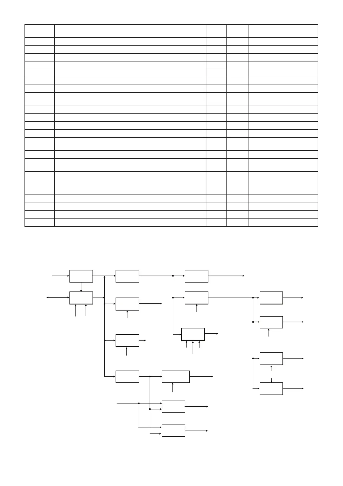
4-5 VOLTAGE BLOCK DIAGRAMS
Voltage from the attached battery pack is routed to the whole of the transceiver via regulators and switches.
LINE
NAME
DESCRIPTION IN/OUT STATUS CONDITION
DASTB1 Strobe signal to the DAC (R: IC950). OUT – –
DASTB2 Strobe signal to the DAC (M: IC600). OUT – –
IOSTB1 Strobe signal to the expander (R: IC951). OUT – –
IOSTB3 Strobe signal to the expanders (M: IC701, 702). OUT – –
IOSTB4 Strobe signal to the expander (L: IC53). OUT – –
APLLSTB Strobe signal to the A BAND PLL IC (M: IC800). OUT – –
BPLSTB Strobe to the B BAND PLL IC (M: IC400). OUT – –
BPS
Power save mode control signal to the A/B BAND PLL ICs (M: IC800/
IC400).
OUT L In power save mode.
UNLK Unlock signal from the A BAND PLL IC (M: IC800). IN H PLL is locked.
CLIN Key detect signal. (Pushed bottom is detected by refering input voltage.) IN A/D –
ATONE Tone signals; tone and WX A BAND. IN A/D –
BTONE Tone signals; tone and WX B BAND. IN A/D –
VIN
DC voltage divided by the voltage detect resisters (L: R159 and R160).
(Remaining battery capacity detection.)
IN A/D –
OPTV External device detect. IN A/D –
TEMP
The voltage in proportion to the internal temperature.
The voltage divided by R66 (thermistor; LOGIC) and R67 (LOGIC).
IN A/D –
S-TXV
• While operated by battery
RSSI voltage from the IF IC (M: IC100).
• While perated by external power supply
Current in TX from the I-V converter (M: IC704).
IN A/D –
BRSSI RSSI voltage from the B BAND IF IC (M: IC200). IN A/D –
CTCOUT CTCSS/DTCS signals. OUT D/A –
DTMF Tone signals; DTMF, EUR tone, OUT D/A –
RESET Reset signal from the reset IC (L:IC100). IN H –
DC-IN VCC +5V +3CPU CPU
DC
SW
SW
REG
V5.5+
V3+
V3+
V3+
R3V
T
Q1000,
D1000, 1001
IC102
Q650−652
Q400,401
IC100
Q800,801,830
IC103
IC101,D101
Q202
Q150−153
D150, 151
TAB
Battery pack
T5
NOCP
CHGH CHGC
TXC
VCOA, B, C
AF PWR AMP
(IC400)
LIGHT
COCVC
COCVB
COCVA
AFON
C3R
V3䇭EBMAV5D
AMBEC
MEDOM
CVD
CODEC CODEC
3V
CHG
MAINR3V
RFR3V
T6
AF6V
REG
DC-DC
LED3V
MODEM3V
REG
+3V
REG
VCO3V
AMBE
REG
4-4 CPU PORT ALLOCATION (continued)