3 - 3
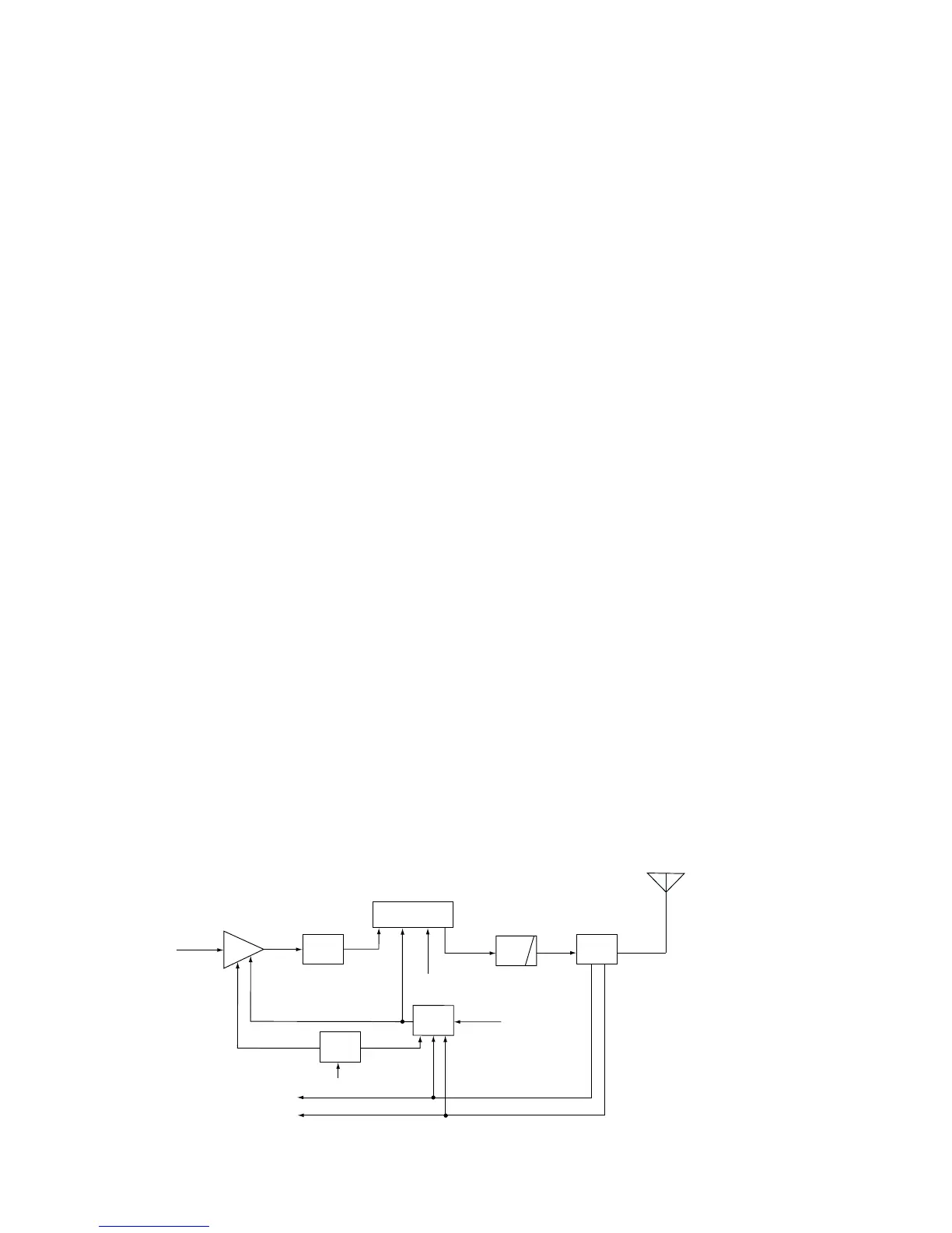
The mixed signals are applied to the splatter filter (IC4).
• INCASE OF THE AF SIGNALS FROM THE ANTENNA
CONNECTOR
The AF signals (received signals) from the antenna connec-
tor (RX unit; J1) are applied to the buffer amplifier (IC9),
CTCSS detector (IC29) and AF amplifier (IC6). The ampli-
fied signals are applied to the D/A converter IC (IC25, pins
8, 9) to adjust a level needed. The adjusted signals pass
through the RPT AF mute switch (IC14), and are applied to
the limiter amplifier (IC3).
• INCASE OF THE 2/5TONE SIGNALS
The 2/5TONE signals from the CPU (IC33, pin 43) are
applied to the limiter amplifier (IC3) via TX signal filter circuit
(IC3, pins 8, 10, 12, 14).
• INCASE OF THE DTMF SIGNALS FROM DIALER
IC
The DTMF from dialer IC (IC47, pin 14) are applied to the
mixer amplifier (IC3) via the TX signal filter circuit (IC3, pins
8, 10, 12, 14).
• INCASE OF THE CTCSS AND DTCS SIGNALS
FROM THE CPU
The CTCSS and DTCS signals from the CPU (IC33, pin 44)
are applied to the TX-tone filter (IC4, pins 12, 14). The fil-
tered signal are applied to the D/A converter IC (TX unit;
IC5) to adjust a tone level needed, and are then mixed with
AF signal at the mixer amplifier IC (TX unit; IC6).
3-2-2 MODULATION CIRCUIT (TX UNIT)
The modulation circuit modulates the VCO oscillating signal
(RF signal) using the AF audio signals.
The filtered signals from the LOGIC unit are applied to the
D/A converter (IC5, pin 4) to adjust AF level. The adjusted
signals are applied to the mixer amplifier IC (IC6, pin 1) with
the CTCSS/DTCS signals.
The mixed signals are applied to the TX VCO circuit to mod-
ulate the oscillated signal (TVCO unit; D5) and modulate the
oscillated signal at VCO circuit (TVCO; Q1, D1–D4). The
modulated VCO output is amplified at the buffer amplifier
(Q1) and is then applied to the drive amplifier circuit on the
PA unit.
3-2-3 POWER AMPLIFIER CIRCUIT (PA UNIT)
The power amplifier circuit amplifies the driver signal to an
output power level.
The RF signal from the TX unit is applied to the pre-drive
(Q4) to amplify the level needed at the power amplifier. The
amplified signal passes through the attenuator circuit
(R29–R31) and is then applied to the power amplifier (IC2).
The RF signal from the pre-drive (Q4) is applied to the
power amplifier (IC2) to obtain 50 W ([EUR2], [FRG2]: 25 W)
of RF power.
The amplified signal is passed through a low-pass filter cir-
cuit (L6, L7, L20, C1–C3, C48, C73, C98, C100) and APC
detector (D2, D4, R7, R8, R20, R21, R25, R26, R29, R36,
R37, C78, C79), and is then applied to the TX antenna con-
nector (CHASSIS; J1).
Control voltage for the pre-drive (Q4) and power amplifier
(IC2) comes from the APC amplifier (IC1, Q9, Q10) to obtain
stable output power. The transmit mute switch (Q7, Q8) con-
trols the pre-drive (Q4) and power amplifier (IC2) when
transmit mute is necessary.
3-2-4 APC CIRCUIT (PA UNIT)
The APC circuit protects the power amplifier from a mis-
matched output load and stabilizes the output power.
The APC detector circuit detects forward signals and reflec-
tion signals at D2 and D4 respectively. The combined volt-
age become minimum level when the antenna impedance is
matched at 50 Ω, and the voltage is increased when it is
mismatched.
The detected voltage is applied to the APC amplifier (IC1 pin
3), and the power setting “PCON” signal from the D/A con-
verter (TX unit; IC5), controlled by the CPU (LOGIC unit;
IC33), is applied to the the APC amplifier (IC1 pin 1) for ref-
erence. When antenna impedance is mismatched, the
detected voltage exceeds the power setting voltage. Then
the output voltage of the APC amplifier IC (IC1, pin 4) con-
trols the input current of the drive amplifier (Q4) and power
amplifier IC (IC2, pin 2) to reduce the output power.