4 - 3
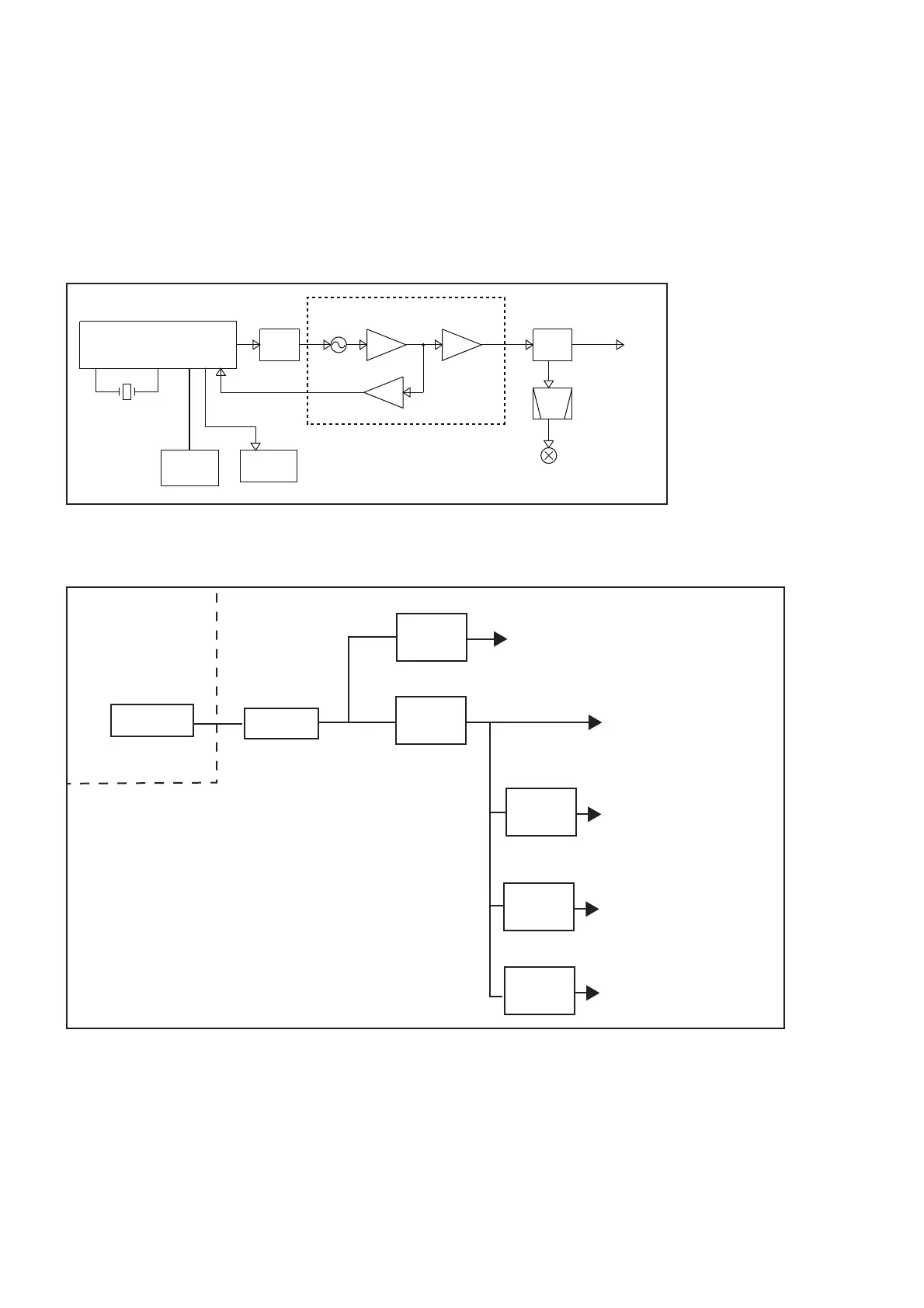
4-3 FREQUENCY SYNTHESIZER CIRCUITS
VCO
While transmitting, the VCO (Q21, 22, D20–23) oscillating
frequency is determined by the value of D22, D23, L22, C26
and C27, and the frequency modulation is carried out by
adding modulation signals to D20.
While receiving, D21 is turned ON and C28 is connected to
the GND to shift the oscillation frequency lower.
The oscillated signals are output via the buffers (Q23, 24).
LO
SW
BPF
BUFFBUFF
BUFF
FIL
LOOP
X1
21.25MHz
1st mixer
D 50,D51
Q24Q23
Q25
Q 21,Q22
IC1
PLL IC
IF IC
CPU
VCO
Q150
TX AMPs
IC170
IC360
PLLO
2ND LO
D22,D23
PLL control signal
PLL
IC1 is a PLL IC which contains prescaler, programmable
counter, phase comparator and charge pump in its package.
The 21.25 MHz reference frequency signal is fed from X1.
The loop fi lter for the VCO is composed by R8, R10, R22,
C11, C13 and C24.
4-4 VOLTAGE BLOCK DIAGRAM
Voltage from the power supply is routed to the whole of the transceiver via regulators and switches.
POWER
CTRL
Q353
VCCHV
R5V
SW
Q221
R5V
V5V
SW
Q220
V5V
T5V
SW
Q222
T5V
5V
regulator
Q224 Q225
S5V
: To TX/RX common circuits
: To RX circuits
: To CPU and EEPROM
: To TX circuits
: To VCO
5V
regulator
IC220
CPU5V
CHASSIS
Battery
MAIN UNIT
• FREQUENCY SYNTHESIZER CIRCUITS
 Loading...