

L
Laura NicholsAug 17, 2025
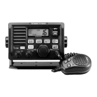
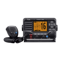
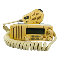
What to do if there is no sound from my Icom Transceiver speaker?
- KKendra HornAug 17, 2025
If you experience little or no sound from your Icom Transceiver speaker, there are several possible reasons. First, the squelch level may be set too high; in this case, set the squelch to the threshold point. Second, the volume level could be set too low; adjust the volume to a suitable level. Finally, if the speaker has been exposed to water, try removing the water using the earthquake function.