Do you have a question about the Icom IC-R100 and is the answer not in the manual?
Specifies the operational frequency ranges for the receiver.
Details the supported receiving modes like AM, FM, WFM.
Lists the available tuning step increments for frequency selection.
States the antenna impedance requirement for optimal performance.
Specifies the necessary DC power input for the receiver.
Indicates the current consumption of the receiver.
Defines the environmental operating temperature limits.
Details the receiver's frequency stability characteristics.
Specifies the capacity for storing memory channels.
Provides the physical dimensions of the receiver unit.
States the overall weight of the receiver unit.
Details the receiver's sensitivity levels for different modes.
Specifies the receiver's selectivity characteristics.
Indicates the maximum audio output power.
States the required audio output impedance.
Identifies components visible on the top side of the receiver.
Identifies components visible on the bottom side of the receiver.
Presents a high-level overview of the receiver's functional blocks.
Describes radio frequency circuits including filters and converters.
Details intermediate frequency circuits for signal processing.
Explains Phase Locked Loop circuits for frequency control.
Covers various voltage regulators and power distribution.
Describes miscellaneous circuits like dimmer and reset.
Details CPU port allocations and logic unit functions.
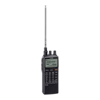
Lists and illustrates the external front panel components.
Details the included accessories supplied with the receiver.
Lists and illustrates internal structural and chassis components.
Component list for the Volume/Squelch control unit.
Component list for the keypad input unit.
Component list for the main logic and CPU unit.
Comprehensive component list for the main receiver board.
Component list for the Phase Locked Loop frequency control unit.
Component lists for the various filter units (FIL 1-4).
Lists required test equipment and preparation steps.
Illustrates the proper connection of test equipment.
Procedures for adjusting PLL reference frequency and LO levels.
Procedures for adjusting 2nd LO and WFM stages.
Procedure for adjusting the overall receiver sensitivity.
Procedure for calibrating the S-meter indicator.
Procedure for adjusting the preamplifier stage.
Procedure for adjusting the Automatic Frequency Control circuit.
Procedure for adjusting the squelch threshold levels.
Illustrates the board layout for Tenkey and VR units.
Illustrates the component layout for the main receiver unit.
Illustrates the component layout for the PLL frequency control unit.
Illustrates the board layouts for the FIL 1-4 units.
Provides a schematic showing voltage levels throughout the circuit.