3·1·23 VSC CIRCUIT (MAIN UNIT)
The
VSC
(Voice Scanning Contral) dele
ct
s the
AF
signal
dUling scanning and skips undesired signaIs such as
unmodulated signaIs. beal signaIs and
nor
se component
signa/s.
The AF signal outpul Irom
Ihe
squelch switch (0 1) passes
Ihrough an
acli
ve lilter circu
il
(ICl a, R6
-R13
,
CG-
Cl 0)
which a
lte
nuates the components of frequencies 1 kHz
and above. The filtered signa' is amplified sulticiently
al
ICl
b and is Ihen detecled at
02.
Tbe detected voltage
is charged at
elS
and is then applied to a comparator
(IC2b). Pin 7 of IC
2b
outputs a " HIGH" signaI only when
receiving AF signaIs.
e15 and R22 set the charge time. The release time is
se
t al R23.
04,
OS
and
OS2
control a relay circuit (R
L1
)
lor
the
[REC REMOTE] jack on
Ihe
REAR
PANEL. RL1 Is turned
ON by the " M
O"
signal
Ir
om Ihe LOGIC UNIT when
receiving AF siqnals.
VS
C operation is given priority even
when the squelch is open. When the
VSC
function is
a
cli
vated, RL1 is turned OFF by the
"M
O" signal trom
tne LOGIC UNIT.
3·1
·24 CENTER DETECTOR AND CENTER
METER CIRCUITS (MAIN UNIT)
The center detector circuit adjusts the center frequencies
ol
Ihe IF signaIs in the WFM and FM demodulator
circuits.
R2
24 adjusts the mismatch of the center frequencies by
using tne offset vollage fr
om
R224, R
22S
and R229.
The center signaI passes through a
De
amplifier
(Q1
7 or
04
3). The amplilied signal is inverted and amplilied at
IC
2a
.
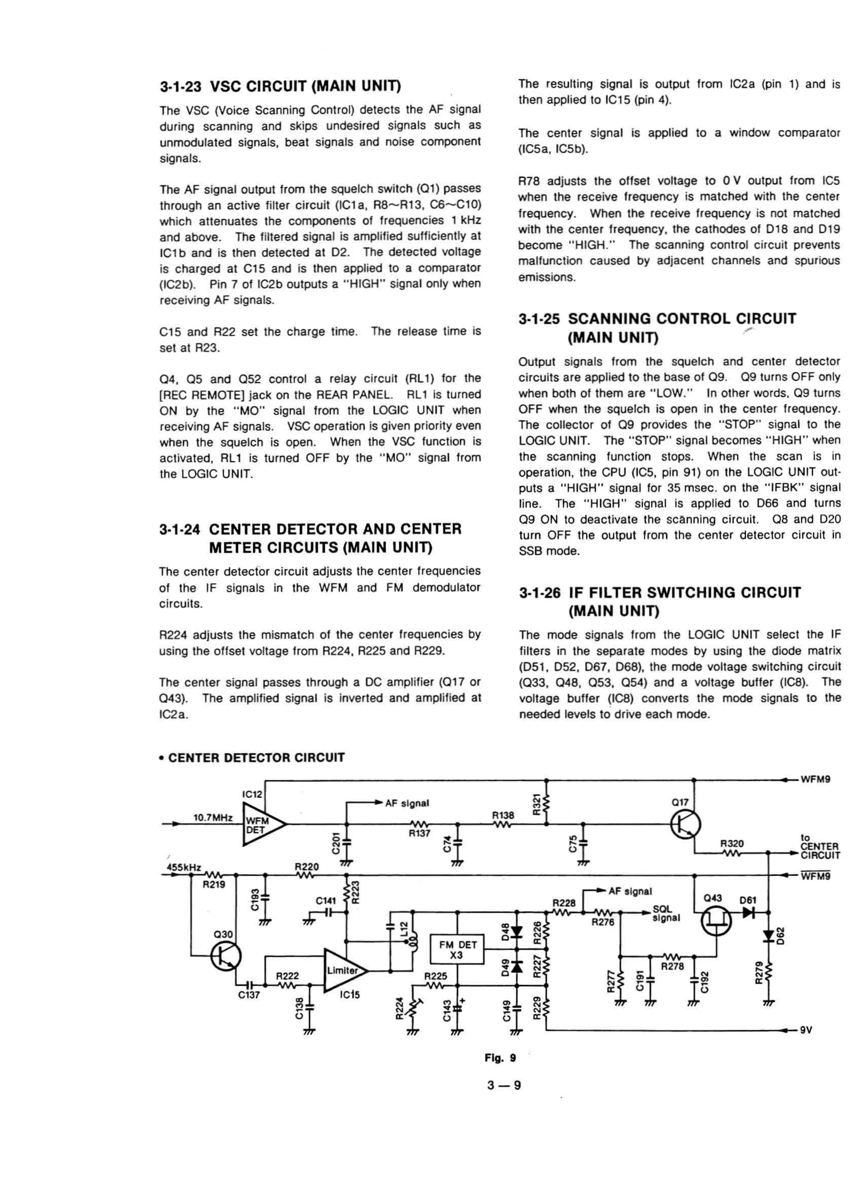
• CENTER DETECTOR CIRCUIT
The resu
l1
ing signaI is output trom IC2a (pin 1) and IS
Ihen applied la I
C1S
(pin 4).
The center signaI is applied
la
a window ce
rn
parator
(ICSa, ICSb).
R76 adjusts tne
olfsel
vollage 10 0 V output from I
CS
when Ihe receive trequency is
mat
ched with the center
frequency. When the receive frequency is not matebeo
with the
center Irequency, Ihe
ca
thodes
ol
0 16 and 0 19
become " HIGH
."
The scanning control circuit prevents
malfunction caused by adjacent channels and spurious
emissions.
3·1·25 SCANNING CONTROL CIRCUIT
,
(MAIN UNIT)
Output signaIs from tne sque
lc
h and center delector
circuits are applied to the base of
0 9. 0 9 turns OFF only
when bath
of
them are
"LOW."
In otner words, 0 9 turns
OFF when the squelch is open in the center frequency.
The coltector of
09
provides the " STOP" signal la Ihe
LOGIC UNIT. The "STOP" signaI becomes
"H
IGH" when
the scanning tunetion stops. When the scan is in
operatlon, Ihe
CP
U (IC
S,
pin 9
1)
on tne LOGIC UNIT out-
puts a
"H
IGH"
signal tor 35 msec. on the " IF
BK"
signal
line. The " HIG
H"
signaI is applied to D66 and turns
Q9 ON 10 deactivate the scanning circuit. Q6 and D20
turn OFF the output from the center detector
circ
uit in
SSB mode.
3-1-26
IF
FILTER SWITCHING CIRCUIT
(MAIN UNIT)
The mode signaIs
Ir
om Ihe LOGIC UNIT select tne IF
filters in the separate modes by using the diode matrix
(OSl,
OS2
,
067
, D66), tne mode voltage switching circuit
(033,
046,
OS3,
OS4
) and a voltage buffer (I
CG).
The
voltage buffer (I
CS
)
co
nv
erts
Ihe
mode signals
la
the
needed l
ev
els to
dr
ive each mode.
W
FM9
IC12
-
........
AF s
lgnal
'"
X;
M
10.7MHz
RI38
a:
WFM
)
DET
R137
-0
fl
1
'"
R320
10
11
1
ö1
CENTE
r
C'RCU
455kHz
R22
0
R2
l9
WFM9
M
M
'"
AF slgnal
~l
'"
0 43
Cl"
1
a:
R228
0
61
,çi
SOl.
h
"I~
'"
R276
slgnal
119
•
03
0
1"
'"
'"
-;~
o '"
'"
FM DET
a:
0
!;>
.....
X3
~
0>
'"
R218
0>
LimIter
..
'"
~
R222
R225
0
a:
r::
-
'"
'"
0>
'"
°l
l~
a:
C137
"-'
C15
,d,.
a:
:!l
0>
M
+
0>
'"
°l
:l!~
..
15
1
'"
-
0
a:
9V
R
IT
FIg. 9
3-9