3·1
RECEIVER CIRCUITS
3·1·1
RF CONVERTER CIRCUIT
(CONV, DOUBLER AND HPF UNITS)
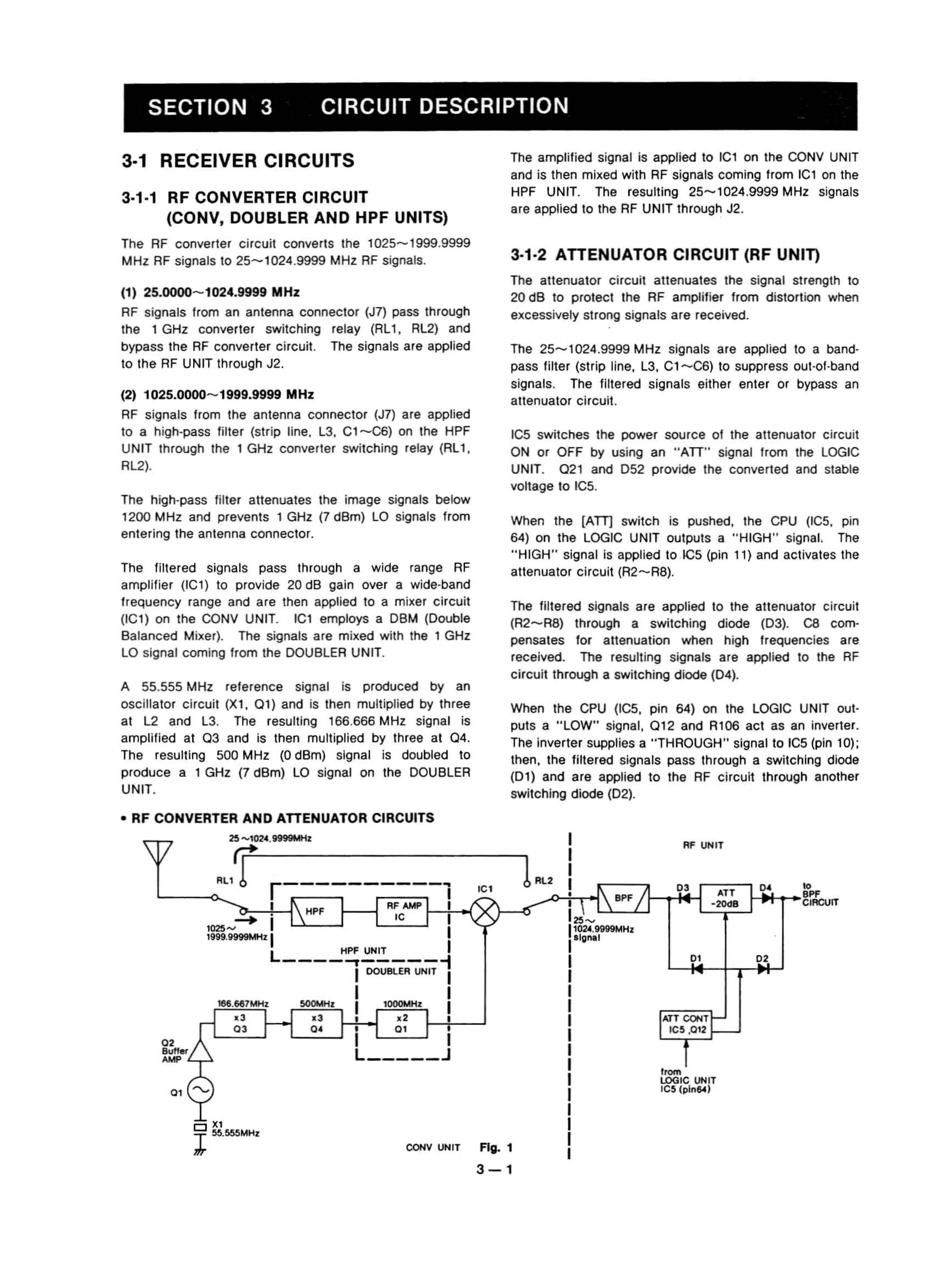
The RF
co
nverter circuit
co
uverts the
1025-1999
.9999
MHz RF siçnats
to
25-1024
.9999 MHz RF signais.
The amplified signal is
ap
p/ied to IC1 on the CONV UNIT
and is then mixed with RF signals coming trom ICt on the
HPF UNIT. The resulting
25- 1024.9999 MHz signais
are applied
to
the RF UNIT through J2.
3·1·2 ATTENUATOR CIRCUIT (RF UNIT)
The high-pass filter attenuates the image signals bel
ow
12
00
MHz and
pr
even
ts
1 GHz (7
dBm
) LO signaIs from
en
te
ring the antenna
co
nnector.
(2) 1025.0000
-1999.9999
MHz
RF signals trom the antenna
co
nnect
or
(J7) are appned
to a high·pass filter (strip fine. L3.
Cl
- C6) on the HPF
UNIT through the 1 GHz converter swi
tc
hing relay (RLt.
RL2).
(1
)
25
.0000
-1024.9999
MHz
RF signals
tr
om an antenna connector (J7) pass t
hr
ough
the 1 GHz converter swi
tc
hing relay (RL1, RL2) and
bypass Ihe RF converter circuit. The signals are applied
to the RF UNIT through J2.
02
RF UNIT
"TT
CONT f-
ICS ,0
12
trom
LOOIC UNIT
IC5
(
pi
n&4)
Tne attenua
tor
circuit attenua
les
Ihe signal strength 10
20
dB
to proteet Ihe RF amplifier trom distortion when
excessively strong signals
are
re
ce
ived.
I
CS
switches Ihe power souree of tne attenuator circuit
ON or OFF by using an
"A
TT" signal trom the LOGIC
UNIT. Q21
an
c DS2 p
ro
vide the converted and stabie
voltage
to
IC5.
When the
[ATT]
swi
tc
h is pushed, the CPU (
ICS.
pin
64) on the LOGIC UNIT outputs a " HIGH" signal. The
" HIGH" signaI is app/ied to !C5 (pin
11
) and activates the
attenu
ato
r circuit (
R2
- R8).
The
fII
tered signals are
app
lied la the
atl
enuator circuit
(
R2-
R8) through a swi
tc
hing diode (D3).
ca
co
rn-
pens
ate
s for attenuati
on
when high f
re
quencies are
receiv
ed
. The resulting signals are applied
to
the RF
circuit through a
sw
itc
hi
ng di
od
e (D4).
When the CPU
(I
CS,
pin 64) on the LOGIC UNIT out-
puts a " LO
W"
signal, Q12 and R10G
act
as an inverter.
The inver
te
r supp/ies a " THROUGH" signal to ICS (pin
10)
;
then, the filtered signals pass through a switchlng diode
(Dl ) and are
ap
pfied to the RF circuit through another
switching diode (02).
The 2
5-
1024.9999 MHz signals are app
/i
ed to a band·
pass filter (strip
fi
ne, L3, Cl - C6) to suppress out-ot-band
signaIs. The flltered signals either enter or bypass an
attenuat
or
circuit.
,
,
I
I
Cl
I
r-"
I-
~
6"
"-<
'i
'
J
1
OPF
(X
l,
t
Ll---L..J
11
024.9999MHz
I
SIQM
!
I
I
,
,
,
,
I
,
I
I
I
I
I
I
CONV
UNIT Fig. 1
500MH'
. 3
O.
166
.667MHz
.3
03
r-
~
0 "
1 55.555MHz
0 1
""'-
02
OU
"
"/
\
AMP '--r
-'
r----------,
L----o.
.......
~JIW
HPF RF
AMP
I
_ " IC I
1025
......
I
"..·....
....
'1
I
L
HPF UNIT
----""'T-----;
I
DO
U
BLER
UNIT I
I I
, '
DOOMH'
,
,
..
I----f'-----'
, Q1 ,
I I
L J
\V
A
55
.555 MHz reierenee signal is produced by an
oscillator circuit
(X
l ,
Ot)
and is then muitiplied by three
at L2 and L3.
Th
e resulting 166.666 MHz signaI is
a
mp
/ified at Q3 and is then multiplied by three at Q4.
The resulting 500 MHz (0 dBm) signal is doubied
to
produce a 1 GHz (7 dBm) LO sig
naion
the OOUBLER
UNIT.
•
RF
CONVERTER
AND
ATIENUATOR
CIRCUITS
The filter
ed
signaIs pass through a wide range RF
amplifier (IC
1)
to provide 20 dB gain over a wide-band
trequen
cv
range ano are then
ap
plled to a mixer
circu
it
(IC1) on the CONV UNIT. ICl employs a OBM (Double
Balanced Mixer). The signals are mixed with the 1 GHz
LO signaI coming trom the OOUBLER UNIT.
3-1