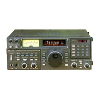
3-2-2 REFERENCE OSCILLATOR CIRCUIT
(PLL UNIT)
The IC-R7100 employs
tw
o reference oscillator c
ir
cuits.
The 51.2 MHz reference oscillator circuit consists of
Q16 and
X2
. The
51
.2 MHz reference frequen
cy
is
appli
ed
to
a bu
lter
amplifier (
02
8). The amplitied signal
enters a buffer amplifier (0 13) or a tripier (
017)
or a 2nd
l O circuit.
The output signal
hom
the V
OO
circuit either passes
Ihrough a three-stage
le
w-pass filter (L59
-L
61, C147-
C152) and is Ihen applied
10 tne P OOUBL UNIT or is
amplifi
ed
al
IC3 and is Ihen applied 10
ICS
to be mixed
with a reference treouency
trom
1C9
.
The resultîng signal trom
Ica
is applied
10
a low
-pa
ss filter
circuit (114,
US
) 10 elimina
te
spurious signals and is tnen
buffer-amplified
al
0 15. The amplified signal is applied
10
Ihe
PLL IC (I
CI.
pin 8).
The reference frequency trom the buffer-amplifier (0 13)
is Ihen divided by 4 al I
CS
aOO
applied 10 Ihe PLL IC
(IC1, pin 1).
The 51.2
MHz refere
nce
frequency Irom Ihe tripter (0 17)
is
app
lied 10 a fil1er
circuil
(L2
5-L2
7)
10
elim
inale
spurious signaIs and is then buffer·amplilied at 0 18. The
amplified signaI passes through the doubler (0 19) and is
app
lied 10 a helical bandpass fi
l1
er (L31. L32)
10
elimina
le
spurious signaIs. The filtered signal is mixed with a
reference freque
ncy
trom Xl and 0 14.
Th
e 12.0 MHz re
ier
enee oscillator circuit consists of
XI and Q4.
The
12.0 MHz reierenee trequency is
genera
le
d at xr and is then multiplied by 3 at Q
14
. The
resulting signal is applied to ICIO
10
be mixed with a
reference freque
ncy
trom X2 anc 0 16.
3·2·5 DOUBLER CIRCUIT (P DOUBLE UNIT)
The VCO oscillation (389.35- 645.84995 MHz) is butter-
amplifi
ed
at IG
lO
and is tnen applied
10
a lew-pass filter
(strip line.
CI68-C
172). The
fil1
ered signal is butter-
amplified at Q2 and Ihen applied
10
a doubler circuit
(01
.02
, L5). The amplitied signal passes Ihrough a band·
pass filter (strip fine. C
113-C
115, C175. C195,
CI
96)
and a
lew
-pass fi
l1er
(strip line, C
I88-C
I 92) 10 sup
pr
ess
u
nw
a
nted
signaIs. The resulting 778.7
-129
1.7 MHz 1si
LO signal is applied
10
Ihe
MI
X1
UNIT
10
produce a 266.7
or
778.7 MHz 1sI IF signa!.
3-2·6 PROGRAMMABLE DIVIDER AND
PHASE DETECTOR CIRCUITS
(PLL UNIT)
The resulting signal trom ICt 0 is butter-amplified at
ICg and is then applied
10
L19
10
eliminate the spurious
signals
and
then
to
ICS
to be mixed with
ve
o output from
Ih
e VCO UNIT.
The programmabie divider shifts the dividing ratio with a
prescaier depending on the operating Irequen
cy
and
determines
Ihe
VCO
oscill
al
ing frequency.
3·2-3
2nd
LO CIRCUIT (PLL UNIT)
The phase detector cir
cu
it
de
tects the off-phase com-
po
nents
ol
the V
OO
frequency using a stabie reference
Irequency.
ICl
is a
one
-chip
Pll
Ie
that contains a two-modulus
pres
ca
ler, a swallow counter, a programmabie divider and
a phase detector.
ICl
accepts
up
to 5
20
MHz inputs.
3·2·7 CHARGE PUMP
AND
LOOP FILTER
CIRCUITS (VCO
AND
PLL UNITS)
The phase·detected signal (
pul
se signal) from
ICI
(pins 15
aOO
16) passes through
Ihe
charge pump (
02,
03
) and is
Ihen
app
lied 10 an
aclive
loop filter
(04-06).
The pulse
signal is converted
10
oe
voltage (PLL voltage) 10 control
oscillation from Ihe
VCO
UNIT. A charge pump (
02
.
03)
is used 10 expand
Ih
e range
of
the PLL loek voltage.
Th
e
PLL loek voltage changes
Ihe
reaetanee
of
Ihe varactor
diodes (0
1-
04,
06
-0
9) in
Ihe
VCO
circuit.
The Inpul signal from PLL IC (IC
l.
pin 8) passes through
the
tw
o-modulus prescai
er
and tne programmabie counter
sec
lion
s
of
IC
I.
A 10 kHz reference tr
eq
uency is applied
10
ICI
(pin 1)
aOO
passes Ihrough a programmabie
reference
cou
nter sec
lio
n of
ICL
Bath
of
the divided
sfgnals
are compared at tne phase detector sec
Uon
of
ICI.
The phase-del
ecled
slgnal (pulse signal) is
OUlpUI
from IC1 (pins 15 and 16).
The 51.2 MHz retere
nc
e signaI is multiplied by 5 at
020
and
is Ihen applied
10
a filter circuit (L36
-L38
) 10
eliminate spurious signaIs. The filtered signal iS then
buffer
-amplified at Q21 and applied 10 the two separate
amplifier circu
it
s.
(1
) 256
.0
MHz
2nd
LO
The
amp
lified signal tr
om
021 is re-amplified al
024
to
obtain a 256.0
MHz
200
LO signa!.
(2) 768
.0
MHz
2nd
LO
The ampl
if
ied signal from 0
21
is multiptled by 3 at 0 22
an
d is
Ihen
applied 10 a helical bandpass filter (L42) 10
eliminate spurlous signaIs. The filtered slgnal Is bu
ff
er-
amplil
ied at
023
10 obta
in
a 768.0 MHz 2nd LO signa
!.
3·2-4 VCO CIRCUIT (VCO UNIT)
The VCO circuit
co
nsists
of
two
VCO
's on Ihe VCO UNIT.
V
COI
(0 1.
02
, 01
-04
) genera
les
Ihe 389.35- 514.3995
1st LO frequency, while the V
C0
2 (
03.
04
,
06
-0
9)
ge
nerates
Ih
e 514
.35-
-645.84995 MHz 1sI LO signa
!.
The
varac
tor diodes
(01-04
,
06
-09)
provide frequency
controt. 3 - 11
Eilher a 256.0
MHz
or
a 768.0 MHz 2nd LO slgnal is
app
lied
to
Ihe
2nd
mixer circuit (IC7) on
Ihe
MIX2 UNIT
10
produce
a 10.7 MHz 2nd IF signa!.
 Loading...