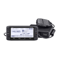
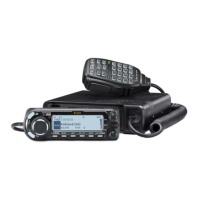
4 - 4
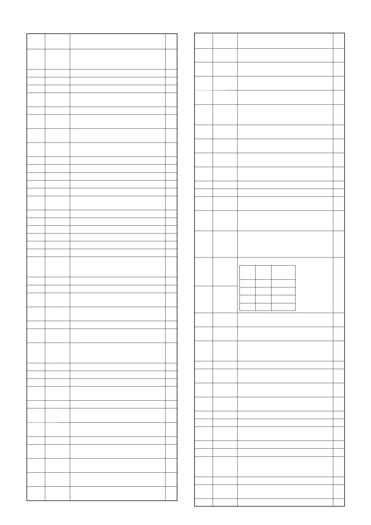
BALL
No.
LINE
NAME
DESCRIPTION I/O
A4 G_RES
GPS module (CHASSIS: EP1) controller
(IC1) reset.
L: Reset.
O
A5 REMOTE HM-75A key input detect. I
A6 VIN External power supply voltage. I
A7 RTONE DV signal/recorded audio. I
A8 TTEMP
TX AMP (MAIN UNIT: Q45) temperature
sensing voltage.
I
A10 DICK1 [DIAL] (outer dial) (S12) phase-A I
A11 UNLK
PLL unlock detect.
L: Unlock is detected.
I
A12 DALD
D/A converter (MAIN UNIT: IC11) strobe.
(“H” and “L” are reversed.)
O
A13,
A14
KS0,
KS2
Key matrix ports. O
B1 DTMF DTMF/European tone/Beep signal. O
B5 LV Lock voltage. I
B7 TXI-V TX current fl ow sensing voltage. I
B8 TEMP Temperature sensing voltage. I
B10 DIUD1 [DIAL] (outer dial) (S12) phase-B I
B11 CLSFT
CPU clock frequency control.
H: The clock frequency is shifted.
O
B13 KS1 Key matrix port. O
B15 KR0 Key input detect. I
C2 CTCSS CTCSS/DTCS tone signal. O
C5 VOX VOX sensing voltage. I
C7 CTCIN CTCSS tone signal input. I
C10 DIUD2 [DIAL] (inner dial) (S12) phase-B. I
C11 DTCS
CTCSS/DTCS fi lter (R65, R68, C78, C80)
switching.
H: DTCS is in use.
O
C13 KS3 Key matrix port. O
C14 KR1 Key input detect. I
C15 DCIN
External power supply connection detect.
L: External DC input.
I
D1 DADATA
D/A converter serial data.
(“H” and “L” are reversed.)
O
D2 G_RXD GPS data input. I
D4 DCSFT
DSP clock frequency control.
L: Clock frequency is shifted.
O
D5 BTSENC
Battery type detect.
( Detecting intermediate voltage of the bat-
tery pack.)
I
D6 BTVIN Battery pack voltage. I
D7 RSSI S-meter voltage. I
D10 DICK2 [DIAL] (inner dial) (S12) phase-A. I
D11 DACK
D/A converter (MAIN UNIT: IC11) clock.
(“H” and “L” are reversed.)
O
D12 KR2 Key input detect. I
D13 BTDET
Battery attachment detect.
L: Battery attached.
I
D14 PWRSW
[POWER] key.
L: Pushed.
I
E4 G_TXD GPS data output. O
F12 CHGC
Charging ON/OFF control.
H: While charging.
O
F13 TXLED
TX LED (DS7) driver (Q9) control.
H: While transmitting.
O
F15 BLED
BUSY LED (DS7) driver (Q8) control.
H: While the squelch is open.
O
G1 RESET
CPU reset.
L: Reset.
I
BALL
No.
LINE
NAME
DESCRIPTION I/O
G3 LIGHT
LCD and key backlight (DS1, DS3) driver
(Q23) control.
O
G4 DIM
LCD backlight (DS1, DS3) dimmer control.
H: Blight.
O
G12 INTMIC
Internal MIC (MAIN UNIT: MC1) control.
H: Internal microphone is in use.
O
G14 CHGH
Charging current control.
H: While charging.
O
G15 PCON
Power lines “PS3” and “5VS” SW (MAIN
UNIT: IC4) control.
H: While the transceiver’s power is ON.
O
H12
VCO_
SEL
VCO power supply control.
L: While the transceiver's power is ON.
O
J4
RTC_
IRQ
Real time clock “IRQ” input. I
J12 MMUTE
MIC mute SW (IC16) control.
L: Mute.
O
J13 TXMUTE
TX mute SW (MAIN UNIT: Q43) control.
H: mute.
O
J15 PFMC GPS/DSP operating mode control. O
K1 NOIS Noise level sensing voltage. I
K4
DSP_
REQ
DSP “REQ” input. I
K12
VCO_
MUTE
Modulation mute SW (MAIN UNIT: Q21)
control.
H: Mute.
O
K13 WN
2nd IF fi lter (MAIN UNIT: FI1 and FI2)
switching control.
L: FI1 is selected. (While in the FM-N or
DV mode.)
O
K14 MIC1
MIC gain control.
MIC1 MIC2
MIC gain
level
LL 4
HL 3
LH 2
HH 1
O
K15 MIC2
L12 SQL
[SQL] (MAIN UNIT: S1) input.
L: Pushed.
I
L14 PS3C
Power line “PS3C” SW (Q13) control.
L: While in the power save mode.
O
L15 R3C
Power line “R3C” SW (MAIN UNIT: Q24)
control.
L: While receiving.
O
M2 CLOUT Cloning data. O
M5
DSP_
STB
DSP (IC18) strobe. O
M6 DSPC
Power line “CVDD_1.35V” SW (IC10) control.
H: While the DSP’s power is ON.
O
M7 PPS
PLL operating mode control.
H: While in the power save mode.
O
M8 LCDRS LCD (DS10) reset. O
M9 LCDCS LCD (DS10) chip select. O
M10
DSP_
REMP
DSP “REC EMP” input. I
M12 TX232 RS-232C serial data output. O
M14 ESIO EEPROM (IC7) serial data. I/O
M15 T3C
Power line “T3C” SW (MAIN UNIT: Q17,
Q19) control.
H: While transmitting.
O
N1 CLIN Cloning data. I
N2
SD_
SENC
SD Card insertion detect.
L: A microSD card is inserted.
I
N3 SD_TXD MicroSD card data output. O
4-5 PORT ALLOCATIONS
• CPU (LOGIC UNIT: IC5)
 Loading...