EasyManua.ls Logo

IDT VersaClock 3S User Manual

IDT VersaClock 3S
12 pages
To Next Page IconTo Next Page
Page #1 background imageLoading...
Page #1 background image
1©2017 Integrated Device Technology, Inc. June 8, 2017
Introduction
The evaluation board is designed to help the customer evaluate the 5P35023 device, the latest addition to the family of programmable
devices in IDT's Timing portfolio. When the board is connected to a PC running IDT Timing Commander™ software through a USB, the
device can be configured and programmed to generate different combinations of frequencies.
Board Overview
Use Figure 1 and Table 1 to identify: USB connector and the input and output frequency SMA connectors.
Figure 1. EVK5P35023 Evaluation Board
4
3
2
1
5
J
I
G
F
E
D
C
B
A
H
User Manual
VersaClock
®
3S - 5P35023 Evaluation Board

Other manuals for IDT VersaClock 3S

Question and Answer IconNeed help?

Do you have a question about the IDT VersaClock 3S and is the answer not in the manual?

IDT VersaClock 3S Specifications

General IconGeneral
TypeProgrammable Clock Generator
Package TypeVFQFPN
CategoryClock Generator
Output TypesLVCMOS
Supply Voltage3.3 V
Operating Temperature Range-40°C to 85°C

Summary

Introduction

Board Overview

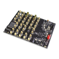
Identifies USB connector and input/output frequency SMA connectors using Figure 1 and Table 1.

Board Power Supply

Power Supply Options

Explains core voltage sources (VDD33, VDDA) and USB power supply for the device.

Output Clock Voltages

Connecting the Board

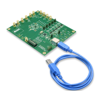
Describes connecting the board to a PC via USB for configuration and programming.

On-board Crystal

Board Default Frequency Output

Lists the default output frequencies for various output ports on the evaluation board.

DIP Switch (SW1)

Configuration and Setup from I2C Port

Step-by-step guide for configuring the board using the Timing Commander software via I2C.

Evaluation Board Schematics

Evaluation Board Schematic (1)

Presents the first part of the evaluation board's electrical schematic diagrams.

Evaluation Board Schematic (2)

FTDI Chip Overview

Details the FTDI chip used for USB communication and its associated pins.

Evaluation Board Schematic (3)

Signal Termination Options

Introduces termination options for differential and single-ended outputs for signal integrity.

Evaluation Board Schematic (4)

Voltage Regulators

Details the voltage regulators (LM317) used for various output voltages on the board.

Signal Termination Options Details

Termination for Differential Output 1

Specifies series resistors and capacitors for LPHCSL differential output 1 (DIFF_T1/C1).

Single-ended Output Termination

Termination for Single-ended Output 1 (SE_1)

Specifies series resistors and capacitors for LVCMOS single-ended output 1 (SE_1).

Revision History

Related product manuals