Do you have a question about the Infineon AURIX TC 4 Series and is the answer not in the manual?
Describes the manual's purpose, features, and hardware details of the AURIX™ TCxx4 lite Kit.
Identifies design, verification, test, and software engineers as the target users.
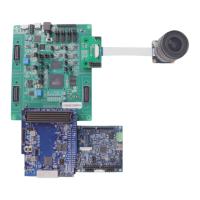
Illustrates the main components and interconnections of the AURIX™ TCxx4 lite Kit.
Details the DC and USB power input options and voltage considerations for the AURIX™ TCxx4 lite Kit.
Describes the on-board user push button, reset button, LEDs, and potentiometer functionality.
Explains debugging via on-board miniWiggler and DAP connector, including USB and serial connections.
Details the reset functionality, including power-on reset and methods to issue a reset signal.
Describes the CAN interface, the TLE9251V transceiver, and pin mapping for CAN signals.
Explains the possibility to assemble external Cypress Semper™ NOR Flash devices.
Describes the option to assemble external serial F-RAM, including connection details and limitations.
Details user startup modes and how they are selected by boot mode index and resistors.
Explains specific configuration signals (HWCFG) and their associated resistors for board setup.
Describes optional resistors that enable/disable or change specific signal functions on the board.
Provides detailed pin mapping for the X1 and X2 expansion connectors on the board.
Details signal mapping for Shield2Go Connectors 1 & 2 and the MikroBus™ connector.
Maps AURIX™ pin functions to Arduino compatible interface standards.
Details the pin assignment and usage of the 10-pin Device Access Port (DAP) debug connector.
The AURIX™ TCxx4 lite Kit is a development system designed to facilitate the use, configuration, and connection of Infineon AURIX™ TCxx4 microcontrollers. This kit is particularly useful for design, verification, test, and software engineers who need to understand the functionality and connections of the AURIX™ TCxx4 lite Kit. It is not intended as a cost or size-optimized reference design.
The AURIX™ TCxx4 lite Kit is built around a 32-Bit Single-Chip AURIX™ TriCore™-based Microcontroller, supporting various devices such as the TC334, TC324, TC234, TC224, or TC214. The kit provides a comprehensive environment for developing and debugging application code. It is compatible with development tools like Infineon's free Eclipse-based IDE AURIX™ Development Studio or the Eclipse-based "FreeEntryToolchain" from HighTec/PLS/Infineon. These tools include a C-Compiler, Multi-core Debugger, and Infineon's low-level driver (iLLD), offering unlimited time and code-size for editing, compiling, and debugging. The FreeEntryToolchain also integrates a source-level UDE debugger from PLS.
The board's core functionality revolves around its microcontroller, which is interfaced with various components to enable a wide range of applications. It includes an on-board miniWiggler for debugging, which connects via a Micro-AB USB interface. For external connections, the board offers expansion connectors (X1, X2) that expose most of the AURIX™ pins, allowing for flexible integration with other hardware. Additionally, it features two Infineon Shield2Go connectors, Arduino-compatible connectors for 3.3V logic levels, and a mikroBUS™ connector, expanding its compatibility with a variety of add-on modules. A dedicated DAP Debug connector is also present for advanced debugging scenarios.
Communication capabilities are provided through a CAN transceiver (TLE9251VSJ from Infineon), enabling the kit to be integrated into CAN networks, which are common in automotive and industrial applications. The CAN node 0 of the TriCore™ device is connected to the transceiver, which operates in a stand-by mode by default and can be switched to normal operating mode by driving the CAN_STB pin low from the CPU.
The kit also supports optional external flash memory, specifically Cypress Semper™ NOR Flash devices (S25HL and S35HL) in SOIC-16 packages. This allows for expanded program and data storage. Similarly, an optional external serial F-RAM (Cypress F-RAM FM25VN10-G and CY15B series) in SOIC-8 packages can be assembled for non-volatile ferroelectric RAM capabilities. Both the optional flash and F-RAM share the same QSPI interface, requiring careful consideration during configuration.
For user interaction and status indication, the board includes a user push-button, a reset push-button, three user LEDs, and a potentiometer for variable analog input. Two green LEDs (LED1 and LED2) are low-active and connected to P00.5 and P00.6, respectively, while a red LED (LED3) is low-active and connected to ESRO, visualizing an emergency stop function. Two additional green LEDs (LED5 and LED6) are used to indicate activities of the on-board miniWiggler, with LED5 (ADBUS4) indicating miniWiggler in use and LED6 (ADBUS7) indicating run status.
The board's power supply is flexible, allowing it to be powered via a DC plug (X3) with a recommended voltage range of +7V to +14V, or via the Micro USB plug (X4) with +5V. A green Power LED (LED4) indicates the presence of the generated 3.3V supply voltage. The board incorporates LDOs (G1 and G2) to regulate voltages, with a maximum output current rating of 1A.
The AURIX™ TCxx4 lite Kit is designed for ease of use in development and evaluation. Its multiple connectivity options allow developers to integrate various peripherals and expansion boards.
Powering the Board: The board can be powered either through the DC plug (X3) or the Micro USB plug (X4). When both are connected, the board prioritizes the DC plug if its voltage is higher than +7V. If the DC plug voltage is between +5.5V and +7V, both sources may contribute. It is crucial to avoid applying additional power to the power pins on the headers (VEXT, +5V, +3V3, VDD_USB) if the board is already powered via USB or DC, as this can damage the LDOs or the board itself. The board is not designed for multiple power sources on the same pins, and doing so risks damage. For external circuits, the power pins can act as outputs, but current draw should be monitored to avoid exceeding USB host capabilities (500mA for USB2.0, 900mA for USB3.0). Using a USB3.0 connection is recommended for better performance.
Debugging: Debugging is a central feature, supported through two main channels: the on-board miniWiggler via the microUSB X4 and a 10-pin DAP Connector. Before connecting the board to a PC for debugging, it is essential to install the latest DAS software. The miniWiggler JDS provides a low-cost debug interface to access the device via DAP. The green LED5 (ADBUS4) indicates a working connection to the DAS server, while LED6 (ADBUS7) shows the debugger's run status. When using the DAP connector, ensure the miniWiggler JDS (LED5) is off to avoid conflicts.
Serial Communication: Upon initial USB connection to a PC, the necessary drivers will be installed automatically, creating a new COM port. This COM port can be used for serial communication with the board via ASCLIN0 (on P14.0 and P14.1) or ASCLIN4 (if R44 and R45 are assembled, primarily for TC3X4 devices). ASCLIN0 is also used for Arduino pins, so if ASCLIN4 is used in parallel, ensure P14.0/P14.1 are not configured for ASCLIN0.
Expansion and Peripherals: The expansion connectors X1 and X2 provide access to most AURIX™ GPIOs and signals, allowing for custom circuit extensions and measurements. The Shield2Go and mikroBUS™ connectors offer compatibility with a wide range of sensor and actuator modules, simplifying prototyping. The Arduino-compatible connectors enable the use of Arduino shields, but it's important to note that the AURIX™ TCxx4 lite Kit operates at 3.3V logic levels, so 5V Arduino boards cannot be directly used. The Arduino connectors support SPI, I2C, UART, PWM outputs, and ADC inputs.
User Interaction: The user push-button (Button1, P00.7) and potentiometer (connected to AN0) provide direct input mechanisms for application development. The reset button (/PORST) allows for manual hardware resets. The LEDs (LED1, LED2, LED3) provide visual feedback on the board's status and application behavior.
Bootmode Configuration: The board's boot mode can be configured using hardware configuration signals (HWCFG[5...3]), which are influenced by optional resistors. This allows developers to select different startup modes, such as internal start from flash or generic bootstrap loader.
The AURIX™ TCxx4 lite Kit incorporates several design considerations that, while not strictly "maintenance," relate to the care and handling of the device to ensure its longevity and proper function.
ESD Precautions: The evaluation board contains components sensitive to electrostatic discharge (ESD). Proper ESD control precautions, such as using ESD-safe workstations and handling procedures, are essential during installation, testing, servicing, or repair to prevent component damage. Referencing applicable ESD protection handbooks and guidelines is recommended.
Thermal Management: During testing, the heat sink and device surfaces of the evaluation board may become hot. Users should take necessary precautions when handling the board to avoid injury. Additionally, the board is shipped with packing materials that must be removed prior to installation. Failure to remove all unnecessary packing materials can lead to overheating or abnormal operating conditions.
Power Supply Management: Careful management of the power supply is critical. As noted, applying multiple power sources to the same pins or exceeding the LDO's maximum output current rating (1A) can damage or destroy the board. Developers should ensure that external power supplies are within the recommended voltage ranges and that current draw from external circuits does not overload the USB host or the board's internal regulators.
Optional Resistor Configuration: The functionality of specific signals can be enabled, disabled, or changed by assembling or removing optional resistors/bridges (e.g., R33 for the potentiometer, R37 for XTAL2, R39 for +5V connection to Mikrobus/Shield2Go, and various HWCFG resistors). This allows for customization of the board's behavior but requires careful attention to the resistor values and their impact on the system. For instance, desoldering R33 disables the potentiometer and frees up AN0 for other uses.
External Flash/F-RAM Assembly: When assembling optional external flash or F-RAM, specific ceramic capacitors and resistors (e.g., C64, R67, R68 for flash; C65 for F-RAM) must also be assembled. It is important to check the datasheets for the chosen F-RAM device, as some may require external pull-up connections for pins like #WP and #HOLD, which are not internally connected on the board. These connections may need to be made via wire wrap lines.
Software Updates: Keeping the DAS software updated is crucial for effective debugging. Users should contact their local FAE or visit the DAS website for the latest software releases.
Environmental Conditions: While the board's design considers environmental conditions, it is primarily for demonstration and evaluation. It is not qualified in terms of safety requirements, manufacturing, or operation over the entire operating temperature range or lifetime. It is the customer's responsibility to ensure that the board is handled in compliance with relevant requirements and standards of the country of operation, especially concerning CE or similar standards. The board is not intended for reliability testing or production.
| ADC Resolution | Up to 12-bit |
|---|---|
| Architecture | TriCore |
| Safety Features | Lockstep cores |
| Communication Interfaces | Ethernet, CAN FD, LIN, SPI, I2C |
| Operating Voltage | 3.3V / 5V |
| Target Applications | Automotive, industrial |
| Package | BGA |