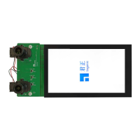
Halley5 Base Board
X2000 Development Kit User Manual
Copyright® 2005-2021 Ingenic Semiconductor Co., Ltd. All rights reserved.
3 Halley5 Base Board
3.1 Configurations of the Halley5 Base Board
Micro USB ports: USB DOWNLOAD/OTG (J2); USB DEBUG for serial (J3).
One Micro SD slot.
One analog MIC, one DMIC port, and one speaker port.
keys and LED indicators
RJ45 Ethernet interface
2 lane MIPI LCD interface
lane / 2 x 2 lane + DVP camera expansion interface
UART/SPI/ADC/PWM expansion interface
3.2 Block Function Description of the Base Board
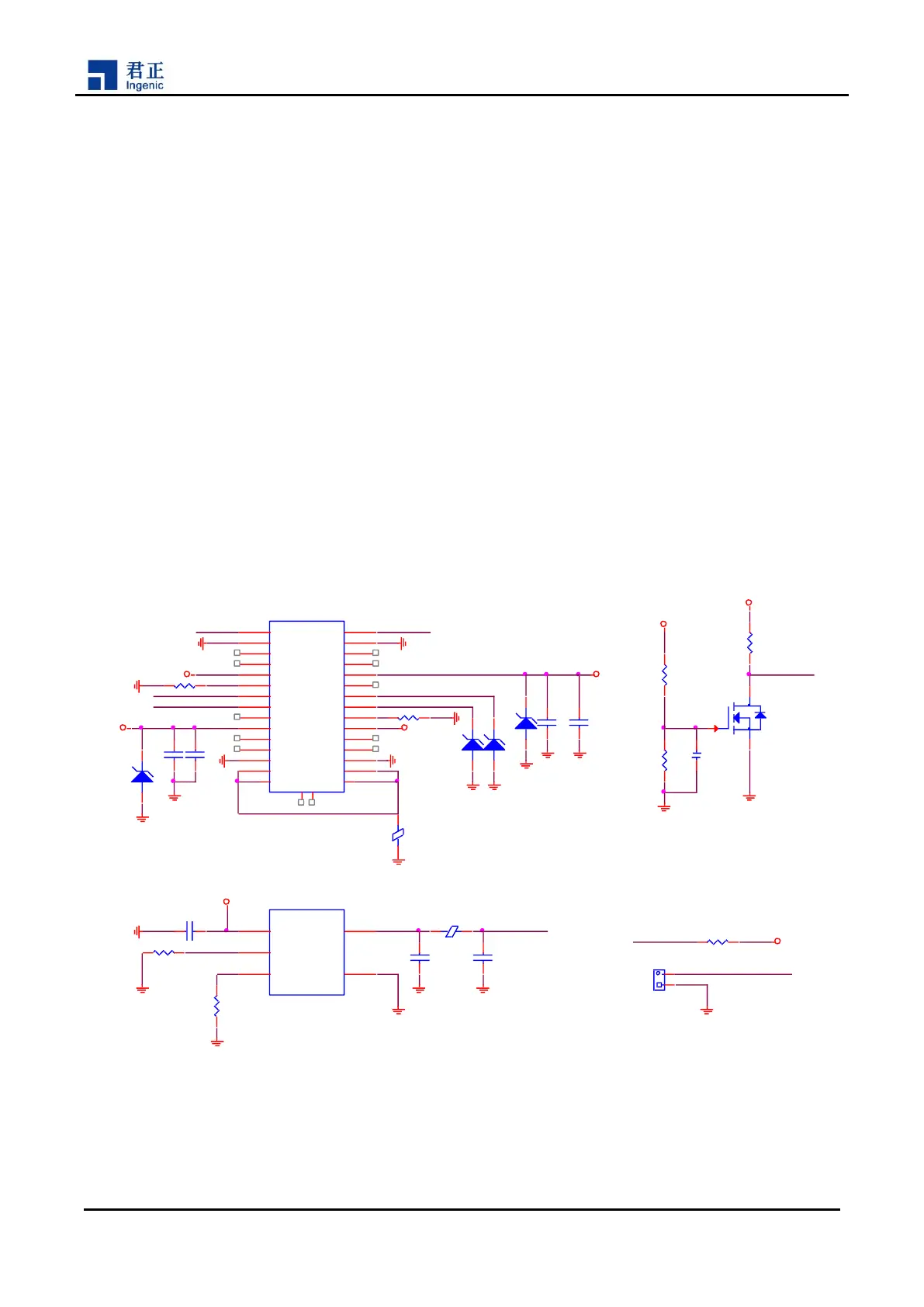
3.2.1 USB OTG function circuit
The TYPE-C port J2 on the Halley5 base board is the download port as well ADB debug port. But if users
cap JP1, J2 will be switched as a USB HOST interface automatically.
Figure 3-1 Halley5 Base Board power supply Circuit
USB_DETECT
R3
100K
R10
100K
C7
0.1uF
USB2.0_OTG
R5
10K
Q1
WNM2306
3
1
2
R13 1K
3V3P
USB_ID
R7 5.1K1%
R9 5.1K1%
R14 100K
FB1
FB
C5
10uF
C6
0.1uF
C3
10uF
C2
0.1uF
SHIELD
J2
SD-105450-001
GND5
A1
TX1+
A2
TX1-
A3
VBUS3
A4
CC1
A5
D1+
A6
D1-
A7
SBU1
A8
VBUS
A9
RX2-
A10
RX2+
A11
GND
A12
GND1
A14
GND4
A13
GND7
B13
GND3
B1
TX2+
B2
TX2-
B3
VBUS1
B4
CC2
B5
D2+
B6
D2-
B7
SBU2
B8
VBUS2
B9
RX1-
B10
RX1+
B11
GND6
B12
GND2
B14
EPD
A15
GND0
A16
NC
A17
NC1
A18
OTG_DM
OTG_DPOTG_DM
OTG_DP
SHIELD
VBUSVBUS
VBUS VBUS
ESD5
ESD9X5VU
1
2
SHIELD
VBUS
JP1
USB_ID
ESD2
ESD9X5VU
1
2
current limit 1A
DRVVBUS
U3
WS4612EAA-5/TR
IN
5
EN
4
ISET
3
OUT
1
GND
2
C10 1uF
DC5V
VBUS
C11
0.01uF
1
2
ESD3
ESD9X5VU
1
2
FB2 FB
R16
6.8K
1
2
1V8P
ESD4
ESD9X5VU
1
2
C576
1uF