5
5
4
4
3
3
2
2
1
1
D D
C C
B B
A A
1. Swapped AD23 and AD19 on 400 pin connector.
2. Separated CSEL on IDE0 and IDE1
3. Swapped pins 1 and 3 (V5 with TP) on CPU-Fan connector.
4. Tied VBAT (pin 65) to 5.0V on Super I/O.
5. Changed RP48 to 4.7K. (Pullups for mouse and keyboard.)
6. Inverted POWERON# signal (SUSC#) from PIIX4 to control soft-on feature.
7. Changed Bulk decoupling on +12 and -12 to 2x220uF from 2x400uF.
8. Changed Bulk decoupling cap C154 from 10uF to 47uF to reduce BOM line items.
Changes made to Revision C.
1. Tied VBAT (pin 65) to 3.3V on Super I/O.
Modular Reference Design
Revision E
History
Changes made to Revision B.
THIS DRAWING CONTAINS INFORMATION WHICH HAS NOT
BEEN VERIFIED FOR MANUFACTURING AS AN END USER
PRODUCT. INTEL IS NOT RESPONSIBLE FOR THE
MISUSE OF THIS INFORMATION.
THIS SCHEMATIC IS PROVIDED "AS IS" WITH NO WARRANTIES WHATSOEVER, INCLUDING
ANY WARRANTY OF MERCHANTABILITY, FITNESS FOR ANY PARTICULAR PURPOSE, OR ANY
WARRANTY OTHERWISE ARISING OUT OF PROPOSAL, SPECIFICATION OR SAMPLE.
No license, express or implied, by estoppel or
otherwise, to any intellectual property rights is
granted herein.
Intel disclaims all liability, including liability
for infringement of any proprietary rights, relating
to use of information in this specification. Intel
does not warrant or represent that such use will not
infringe such rights.
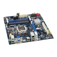
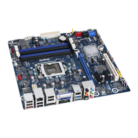
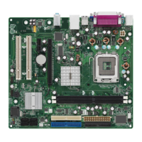
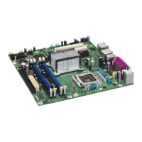
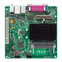
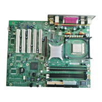
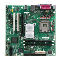
System Electronics Board
Changes made to Revision D.
1. Added Signals PWROK(A24) +12V(A33) MB12#_R(B33) to J19A.
2. Moved J20
3. Added C229 to -PCIRST
Changes made to Revision E.
1. Removed CS_B#[5:0]. Tied CS_Bn# to CS_An# at DIMM
connectors.
2. Changed WE_B#, SCAS_B# and SRAS_B# to WE_A#, SCAS_A#, SRAS_A# on J17
3. Changed WE_A#, SCAS_A# and SRAS_A# to WE_B#, SCAS_B# and SRAS_B# on J16.
4. Pin K25 of the CPU connector has been changed from reserved to VCC_CMOS.
5. A20M#, INIT, SLP, IGNNE NMI,INTR, STPCLK# and SMI are now pulled
up to VCC_CMOS.
6. A20M#, INIT, SLP, IGNNE NMI,INTR, STPCLK# and SMI have series
resistors and 680 ohm pullups from 2.7K pullups.
7. Removed Pullup on FERR#. Processor assembly or interposer
cards must pull this signal up.
8. Modified Boot Block flash to support 28F004B5.
9. Removed Series resistor from MAB12#. Processor Assembly must configure BX FSB
frequency.
10. Removed flash daughter card from schematics.
12. Removed FQS pullups(formerly MAB12#_R).
13. Added R308 as series termination on BXDCLKO.
14. Update RTC Crystal section.
11. Changed MAB12#_R net to FQS.
15. Removed speaker connector.
16. Pin names A01-A09 changed to A1-A9 on ISA and DIMM connectors
17. Changed FB1-FB4, FB9 part # to BLM41P750S, 75 Ohm/100 MHz/3 A
E
Changes
C
122Friday, February 16, 2001
Title
Size Document Number Rev
Date: Sheet of