Technical Reference
59
2.8.2.4 Add-in Board and Peripheral Interface Connectors
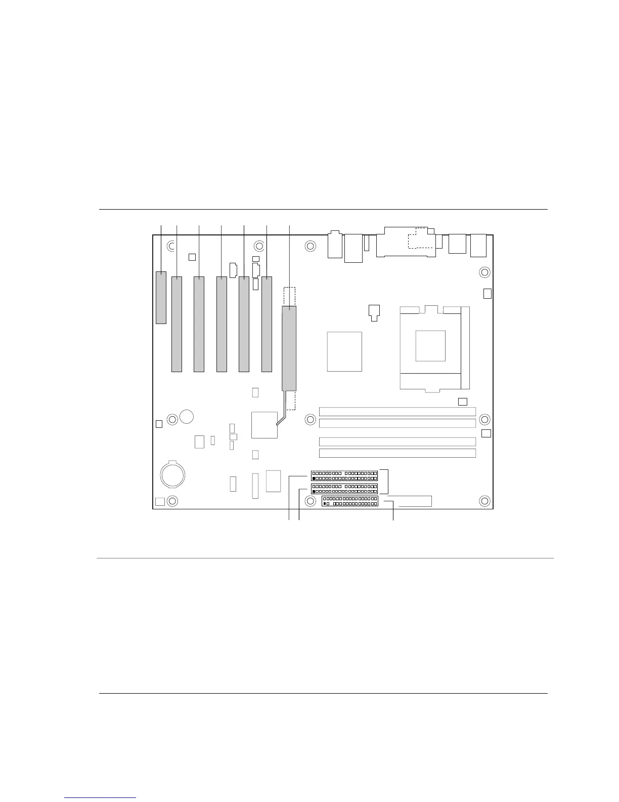
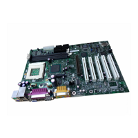
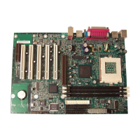
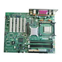
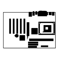
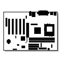
Figure 11 shows the location of the add-in board connector and peripheral connectors. Note the
following considerations for the PCI bus connectors:
• All of the PCI bus connectors are bus master capable.
• PCI bus connector 2 has SMBus signals routed to it. This enables PCI bus add-in boards with
SMBus support to access sensor data on the board. The specific SMBus signals are as follows:
The SMBus clock line is connected to pin A40
The SMBus data line is connected to pin A41
OM10446
1
2
33
34
H
1
240
39
1
240
39
IJ
C D EA B F G
Item Description Reference Designator For more information see:
A Communication and networking riser (CNR) J3A1 Table 38
B PCI bus connector 5 J4A1 Table 39
C PCI bus connector 4 J4B1 Table 39
D PCI bus connector 3 J4C1 Table 39
E PCI bus connector 2 J4D1 Table 39
F PCI bus connector 1 J4E1 Table 39
G AGP connector J5E1 Table 40
H Diskette drive J10G1 Table 42
I Primary IDE J9G2 Table 41
J Secondary IDE J9G1 Table 41
Figure 11. Add-in Board and Peripheral Interface Connectors