Table 7. Pin Migration Conditions for ADC Migration
Source Target Migratable Pins
Single ADC device Single ADC device You can migrate all ADC input pins
Dual ADC device Dual ADC device
Single ADC device Dual ADC device • One dedicated analog input pin.
• Eight dual function pins from the ADC1 block of the
source device to the ADC1 block of the target device.
Dual ADC device Single ADC device
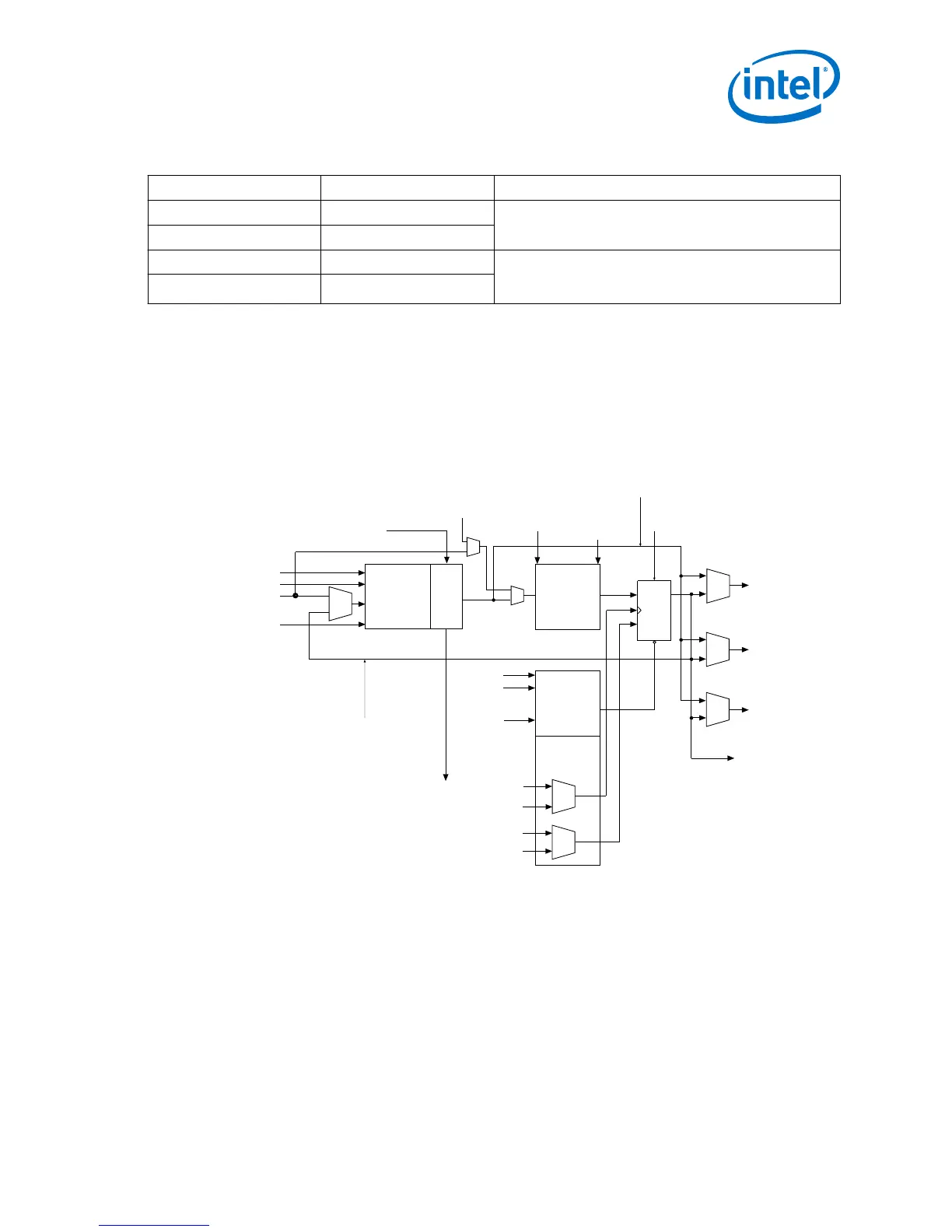
1.7 Logic Elements and Logic Array Blocks
The LAB consists of 16 logic elements (LE) and a LAB-wide control block. An LE is the
smallest unit of logic in the MAX 10 device architecture. Each LE has four inputs, a
four-input look-up table (LUT), a register, and output logic. The four-input LUT is a
function generator that can implement any function with four variables.
Figure 4. MAX 10 Device Family LEs
Row, Column,
And Direct Link
Routing
data 1
data 2
data 3
data 4
labclr1
labclr2
Chip-Wide
Reset
(DEV_CLRn)
labclk1
labclk2
labclkena1
labclkena2
LE Carry-In
LAB-Wide
Synchronous
Load
LAB-Wide
Synchronous
Clear
Row, Column,
And Direct Link
Routing
Local
Routing
Register Chain
Output
Register Bypass
Programmable
Register
Register Chain
Routing from
previous LE
LE Carry-Out
Register Feedback
Synchronous
Load and
Clear Logic
Carry
Chain
Look-Up Table
(LUT)
Asynchronous
Clear Logic
Clock &
Clock Enable
Select
D
Q
ENA
CLRN
1.8 Analog-to-Digital Converter
MAX 10 devices feature up to two ADCs. You can use the ADCs to monitor many
different signals, including on-chip temperature.
1 MAX
®
10 FPGA Device Overview
MAX 10 FPGA Device Overview
9