EasyManua.ls Logo

Intel MAX 10 FPGA User Manual

Intel MAX 10 FPGA
14 pages
To Next Page IconTo Next Page
To Previous Page IconTo Previous Page
Page #8 background image
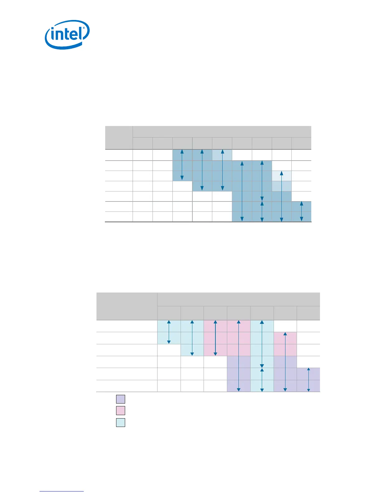
1.6.1 MAX 10 I/O Vertical Migration Support
Figure 2. Migration Capability Across MAX 10 Devices
The arrows indicate the migration paths. The devices included in each vertical
migration path are shaded. Some packages have several migration paths. Devices
with lesser I/O resources in the same path have lighter shades.
To achieve the full I/O migration across product lines in the same migration path,
restrict I/Os usage to match the product line with the lowest I/O count.
Device
Package
V36 V81 M153 U169 U324 F256 E144 F484 F672
10M02
10M04
10M08
10M16
10M25
10M40
10M50
Note: To verify the pin migration compatibility, use the Pin Migration View window in the
Quartus Prime software Pin Planner.
1.6.2 MAX 10 ADC Vertical Migration Support
Figure 3. ADC Vertical Migration Across MAX 10 Devices
The arrows indicate the ADC migration paths. The devices included in each vertical
migration path are shaded.
Device
Package
M153 U169 U324 F256 E144 F484 F672
10M04
10M08
10M16
10M25
10M40
10M50
Dual ADC Device: Each ADC (ADC1 and ADC2) supports 1 dedicated analog input pin and 8 dual function pins.
Single ADC Device: Single ADC that supports 1 dedicated analog input pin and 16 dual function pins.
Single ADC Device: Single ADC that supports 1 dedicated analog input pin and 8 dual function pins.
1 MAX
®
10 FPGA Device Overview
MAX 10 FPGA Device Overview
8
Question and Answer IconNeed help?

Do you have a question about the Intel MAX 10 FPGA and is the answer not in the manual?

Intel MAX 10 FPGA Specifications

General IconGeneral
Device FamilyMAX 10
CategoryFPGA
Technology Node55 nm
Maximum Operating FrequencyUp to 450 MHz
Logic Elements2, 000 to 50, 000
Power Supply1.2V
DSP BlocksUp to 144 18x18 multipliers
Voltage Support1.2V, 3.3V
ConfigurationFlash-based
Operating Temperature0°C to 85°C (commercial), -40°C to 100°C (industrial)
Process TechnologyEmbedded Flash Memory Technology

Summary

MAX 10 FPGA Device Overview

Key Advantages of MAX 10 Devices

Summarizes key benefits and supporting features of MAX 10 devices.

Summary of MAX 10 Device Features

Provides an overview of the device's core technical features and capabilities.

MAX 10 Device Ordering Information

Details on how to order MAX 10 devices, including part numbers and options.

MAX 10 Device Maximum Resources

Table detailing the maximum resource counts for different MAX 10 device variants.

MAX 10 Devices I/O Resources Per Package

Information on I/O pin counts and package types for MAX 10 devices.

MAX 10 Vertical Migration Support

Guidance on migrating designs between different MAX 10 device densities.

MAX 10 I/O Vertical Migration Support

Specifics on I/O migration paths across MAX 10 devices and packages.

MAX 10 ADC Vertical Migration Support

Specifics on ADC migration paths across MAX 10 devices and packages.

Logic Elements and Logic Array Blocks

Explanation of the fundamental logic units (LEs and LABs) in the architecture.

Analog-to-Digital Converter

Details on the integrated Analog-to-Digital Converters (ADCs) and their features.

User Flash Memory

Information on the on-chip non-volatile user flash memory (UFM) capabilities.

Embedded Multipliers and Digital Signal Processing Support

Features related to embedded multipliers and Digital Signal Processing (DSP).

Embedded Memory Blocks

Description of the M9K embedded memory blocks and their configuration options.

Clocking and PLL

Details on clocking resources, global clock networks, and Phase-Locked Loops (PLLs).

FPGA General Purpose I/O

Information on the programmable general-purpose I/O features and flexibility.

External Memory Interface

Description of the external memory interface capabilities, including supported standards.

Configuration

Overview of device configuration features, security, and data compression.

Power Management

Details on power management options, advantages, and controller schemes.

Document Revision History for MAX 10 FPGA Device Overview

History of changes and updates made to the MAX 10 FPGA Device Overview document.

Related product manuals